
Data Sheet

MPU-9250 Product Specification
Document Number: PS-MPU-9250A-01
Revision: 1.0
Release Date: 01/17/2014
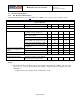
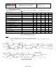
3.4.2 A.C. Electrical Characteristics
Typical Operating Circuit of section 4.2
, VDD = 2.5V, VDDIO = 2.5V, T
A
=25°C, unless otherwise noted.
Parameter
Conditions
MIN
TYP
MA X
Units
Supply Ramp Time
Monotonic ramp. Ramp rate
is 10% to 90% of the final
value
0.1
100 ms
Operating Range
Ambient
-40
85 °C
Sensitivity
Untrimmed
333.87
LSB/°C
Room Temp Offset
21°C
0
LSB
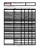
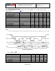
Supply Ramp Time (T
RA MP
)
Valid pow er-on RESET
0.01
20
100
ms
Start-up time for register read/write
From pow er-up
11 100 ms
I
2
C ADDRESS
AD0 = 0
AD0 = 1
1101000
1101001
V
IH
, High Level Input Voltage
0.7*V DDIO
V
V
IL
, Low Level Input Voltage
0.3*VDDIO
V
C
I
, Input Capacitance
< 10
pF
V
OH
, High Level Output Voltage
R
LOAD
=1MΩ;
0.9*VDDIO
V
V
OL1
, LOW-Level Output Voltage
R
LOAD
=1MΩ;
0.1*VDDIO
V
V
OL.INT1
, INT Low -Level Output Voltage
OPEN=1, 0.3mA sink
Current
0.1
V
Output Leakage Current
OPEN=1
100
nA
t
INT
, INT Pulse Width
LA TCH_INT_EN=0
50
µs
V
IL
, LOW Level Input Voltage
-0.5V
0.3*VDDIO
V
V
IH
, HIGH-Level Input Voltage
0.7*VDDIO
VDDIO +
0.5V
V
V
hys
, Hysteresis
0.1*VDDIO
V
V
OL
, LOW-Level Output Volt age
3mA sink current
0
0.4
V
I
OL
, LOW-Level Output Current
V
OL
=0.4V
V
OL
=0.6V
3
6
mA
mA
Output Leakage Current
100
nA
t
of
, Out put Fall Time from V
IHmax
to V
ILmax
C
b
bus capacitance in pf
20+0.1C
b
250
ns
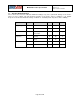
V
IL
, LOW-Level Input Voltage
-0.5V
0.3*VDDIO
V
V
IH
, HIGH-Level Input Voltage
0.7* VDDIO
VDDIO +
0.5V
V
V
hys
, Hysteresis
0.1* VDDIO
V
V
OL1
, LOW-Level Output Voltage
VDDIO > 2V; 1mA sink
current
0
0.4
V
V
OL3
, LOW-Level Output Voltage
VDDIO < 2V; 1mA sink
current
0
0.2* VDDIO
V
I
OL
, LOW-Level Output Current
V
OL
= 0.4V
V
OL
= 0.6V
3
6
mA
mA
Output Leakage Current
100
nA
t
of
, Output Fall Time from V
IHmax
to V
ILm ax
C
b
bus capacitance in pF
20+0.1C
b
250
ns
Sample Rate
Fchoice=0,1,2
SMPLRT_DIV =0
32 kHz
Fchoice=3;
DLPFCFG=0 or 7
SMPLRT_DIV =0
8 kHz
Fchoice=3;
DLPFCFG=1,2,3,4,5,6;
SMPLRT_DIV =0
1 kHz
Clock Frequency Initial Tolerance
CLK_SEL=0, 6; 25°C
-2
+2
%
Page 12 of 42