
Data Sheet

MPU-9250 Product Specification
Document Number: PS-MPU-9250A-01
Revision: 1.0
Release Date: 01/17/2014
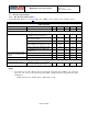
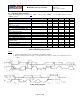
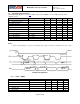
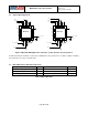
4.2 Typical Operating Circuit
AUX_CL
VDDIO
AD0/SDO
REGOUT
FSYNC
INT
GND
SCL / SCLK
nCS
RESV
VDD
SDA / SDI
NC
2.4 – 3.3VDC
C2, 0.1 µF
C3, 10 nF
1.8 – 3.3VDC
SCL
VDDIO
SDA
AUX_DA
AD0
C1, 0.1 µF
RESV
NC
NC
NC
RESV
NC
NC
NC
NC
NC
MPU-9250
1
2
3
4
5
6
13
18
17
16
15
14
7
8
9
10
11
12
24
23
22
21
20
19
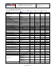
AUX_CL
VDDIO
AD0/SDO
REGOUT
FSYNC
INT
GND
SCL / SCLK
nCS
RESV
VDD
SDA / SDI
NC
2.4 – 3.3VDC
C2, 0.1 µF
C3, 10 nF
1.8 – 3.3VDC
SCLK
SDI
AUX_DA
SD0
C1, 0.1 µF
RESV
NC
NC
NC
RESV
NC
NC
NC
NC
NC
MPU-9250
1
2
3
4
5
6
13
18
17
16
15
14
7
8
9
10
11
12
24
23
22
21
20
19
nCS
(a) (b)
Figure 2 MPU-9250 QFN Application Schematic: (a) I2C operation, (b) SPI operation
Note that the INT pin should be connected to a GPIO pin on the system processor that is capable of waking
the system processor from suspend mode.
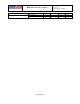
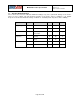
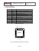
4.3 Bill of Materials for External Components
Component
Label
Specification
Quantity
Regulator Filter Capacitor C1 Ceramic, X7R, 0.1µF ±10%, 2V 1
VDD Bypass Capacitor C2 Ceramic, X7R, 0.1µF ±10%, 4V 1
VDDIO Bypass Capacitor C3 Ceramic, X7R, 10nF ±10%, 4V 1
Table 10 Bill of Materials
Page 20 of 42