
Data Sheet

MPU-9250 Product Specification
Document Number: PS-MPU-9250A-01
Revision: 1.0
Release Date: 01/17/2014
4 Applications Information
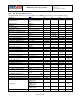
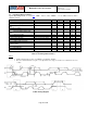
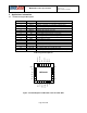
4.1 Pin Out and Signal Description
Pin Number
Pin Nam e
Pin Description
1
RESV
Reserved. Connect to VDDIO.
7
AUX_CL
I
2
C Master serial clock, for connecting to external sensors
8
VDDIO
Digital I/O supply voltage
9
AD0 / SDO
I
2
C Slave Address LSB (AD0); SPI serial data output (SDO)
10
REGOUT
Regulator filter capacitor connection
11
FSY NC
Frame synchronization digital input. Connect to GND if unused.
12
INT
Interrupt digital output (totem pole or open-drain)
13
VDD
Pow er supply voltage and Digital I/O supply voltage
18
GND
Pow er supply ground
19
RESV
Reserved. Do not connect.
20
RESV
Reserved. Connect to GND.
21
AUX_DA
I
2
C master serial data, for connecting to external sensors
22
nCS
Chip select (SPI mode only)
23
SCL / SCLK
I
2
C serial clock (SCL); SPI serial clock (SCLK)
24
SDA / SDI
I
2
C serial data (SDA); SPI serial data input (SDI)
2 – 6, 14 - 17
NC
Not internally connected. May be used for PCB trace routing.
Table 9 Signal Descriptions
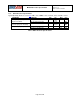
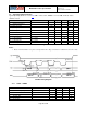
AUX_CL
VDDIO
AD0/SDO
REGOUT
FSYNC
INT
GND
SCL / SCLK
nCS
RESV
VDD
SDA / SDI
NC
AUX_DA
RESV
NC
NC
NC
RESV
NC
NC
NC
NC
NC
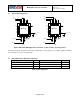
MPU-9250
1
2
3
4
5
6
13
18
17
16
15
14
7
8
9
10
11
12
24
23
22
21
20
19
Figure 1 Pin Out Diagram for MPU-9250 3.0x3.0x1.0mm QFN
Page 19 of 42