
Data Sheet

MPU-9250 Product Specification
Document Number: PS-MPU-9250A-01
Revision: 1.0
Release Date: 01/17/2014
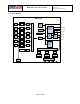
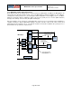
4.20 Bias and LDO
The bias and LDO section generates the internal supply and the reference voltages and currents required by
the MPU-9250. Its two inputs are an unregulated VDD and a VDDIO logic reference supply voltage. The
LDO output is bypassed by a capacitor at REGOUT. For further details on the capacitor, please refer to the
Bill of Materials for External Components.
4.21 Charge Pump
An on-chip charge pump generates the high voltage required for the MEMS oscillators.
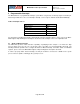
4.22 Standard Power Mode
The following table lists the user-accessible power modes for MPU-9250.
Mode
Name
Gyro
Accel
Magnetometer
DMP
1
Sleep Mode
Off
Off
Off
Off
2
Standby Mode
Drive On
Off
Off
Off
3
Low-Power Accelerometer Mode
Off
Duty-Cycled
Off
On or Off
4
Low-Noise Accelerometer Mode
Off
On
Off
On or Off
5
Gyroscope Mode
On
Off
Off
On or Off
6
Magnetometer Mode
Off
Off
On
On or Off
7
Accel + Gyro Mode
On
On
Off
On or Off
8
Accel + Magnetometer Mode
Off
On
On
On or Off
9
9-Axis Mode
On
On
On
On or Off
Note s:
1. Power consumption for individual modes can be found in Electrical Characteristics section.
4.23 Power Sequencing Requirements and Power on Reset
During power up and in normal operation, VDDIO must not exceed VDD. During power up, VDD and VDDIO
must be monotonic ramps. As stated in Table 4, the minimum VDD rise time is 0.1ms and the maximum rise
time is 100 ms. Valid gyroscope data is available 35 ms (typical) after VDD has risen to its final voltage from
a cold start and valid accelerometer data is available 30 ms (typical) after VDD has risen to its final voltage
assuming a 1ms VDD ramp from cold start. Magnetometer data is valid 7.3ms (typical) after VDD has risen
to its final voltage value from a cold start.
Page 28 of 42