
Data Sheet

MPU-9250 Product Specification
Document Number: PS-MPU-9250A-01
Revision: 1.0
Release Date: 01/17/2014
7 Digital Interface
7.1 I2C and SPI Serial Interfaces
The internal registers and memory of the MPU-9250 can be accessed using either I
2
C at 400 kHz or SPI at
1MHz. SPI operates in four-wire mode.
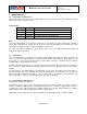
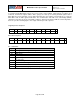
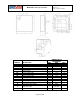
Serial Interface
Pin Number
Pin Nam e
Pin Description
8
VDDIO
Digital I/O supply voltage.
9
AD0 / SDO
I
2
C Slave Address LSB (AD0); SPI serial data output (SDO)
23
SCL / SCLK
I
2
C serial clock (SCL); SPI serial clock (SCLK)
24
SDA / SDI
I
2
C serial data (SDA); SPI serial data input (SDI)
Note:
To prevent switching into I
2
C mode when using SPI, the I
2
C interface should be disabled by setting the
I2C_IF_DIS configuration bit. Setting this bit should be performed immediately after waiting for the time
specified by the “Start-Up Time for Register Read/Write” in Section 6.3.
For further information regarding the I2C_IF_DIS bit, please refer to the MPU-9250 Register Map and
Register Descriptions document.
7.2 I2C Interface
I
2
C is a two-wire interface comprised of the signals serial data (SDA) and serial clock (SCL). In general, the
lines are open-drain and bi-directional. In a generalized I
2
C interface implementation, attached devices can
be a master or a slave. The master device puts the slave address on the bus, and the slave device with the
matching address acknowledges the master.
The MPU-9250 always operates as a slave device when communicating to the system processor, which thus
acts as the master. SDA and SCL lines typically need pull-up resistors to VDD. The maximum bus speed is
400 kHz.
The slave address of the MPU-9250 is b110100X which is 7 bits long. The LSB bit of the 7 bit address is
determined by the logic level on pin AD0. This allows two MPU-9250s to be connected to the same I
2
C bus.
When used in this configuration, the address of the one of the devices should be b1101000 (pin AD0 is logic
low) and the address of the other should be b1101001 (pin AD0 is logic high).
7.3 I2C Communications Protocol
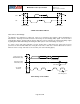
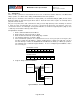
START (S) and STOP (P) Conditions
Communication on the I
2
C bus starts when the master puts the START condition (S) on the bus, which is
defined as a HIGH-to-LOW transition of the SDA line while SCL line is HIGH (see figure below). The bus is
considered to be busy until the master puts a STOP condition (P) on the bus, which is defined as a LOW to
HIGH transition on the SDA line while SCL is HIGH (see figure below).
Additionally, the bus remains busy if a repeated START (Sr) is generated instead of a STOP condition.
Page 32 of 42