
Data Sheet

MPU-9250 Product Specification
Document Number: PS-MPU-9250A-01
Revision: 1.0
Release Date: 01/17/2014
7.5 SPI Interface
SPI is a 4-wire synchronous serial interface that uses two control lines and two data lines. The MPU-9250
always operates as a Slave device during standard Master-Slave SPI operation.
With respect to the Master, the Serial Clock output (SCLK), the Serial Data Output (SDO) and the Serial
Data Input (SDI) are shared among the Slave devices. Each SPI slave device requires its own Chip Select
(CS) line from the master.
CS goes low (active) at the start of transmission and goes back high (inactive) at the end. Only one CS line
is active at a time, ensuring that only one slave is selected at any given time. The CS lines of the non-
selected slave devices are held high, causing their SDO lines to remain in a high-impedance (high-z) state
so that they do not interfere with any active devices.
SPI Operational Features
1. Data is delivered MSB first and LSB last
2. Data is latched on the rising edge of SCLK
3. Data should be transitioned on the falling edge of SCLK
4. The maximum frequency of SCLK is 1MHz
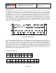
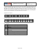
5. SPI read and write operations are completed in 16 or more clock cycles (two or more bytes). The
first byte contains the SPI Address, and the following byte(s) contain(s) the SPI data. The first
bit of the first byte contains the Read/Write bit and indicates the Read (1) or Write (0) operation.
The following 7 bits contain the Register Address. In cases of multiple-byte Read/Writes, data is
two or more bytes:
SPI Address format
MSB
LSB
R/W
A6
A5
A4
A3
A2
A1
A0
SPI Data format
MSB
LSB
D7
D6
D5
D4
D3
D2
D1
D0
6. Supports Single or Burst Read/Writes.
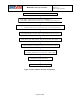
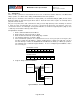
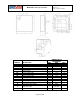
Typical SPI Master / Slave Configuration
SPI Master
SPI Slave 1
SPI Slave 2
/CS1
/CS2
SCLK
SDI
SDO
/CS
SCLK
SDI
SDO
/CS
Page 36 of 42