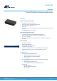
VL53L4CD Datasheet Time-of-Flight high accuracy proximity sensor Features High accuracy proximity ranging • • • • • • High performance proximity sensor From 0 to 1300 mm with full field of view (FoV) Short distance linearity down to 1 mm FoV of 18° Autonomous low power mode with programmable interrupt threshold to wake up the host Fast ranging frequency up to 100 Hz Fully integrated miniature module • • • • 940 nm invisible laser emitter (VCSEL) and analog driver Low power microcontroller running advan
VL53L4CD Description Specifically designed for proximity and short-range measurements, the VL53L4CD provides very accurate distance measurements from only 1 mm up to 1300 mm. A new generation laser emitter with 18° FoV improves performances under ambient light, with ranging speed up to 100 Hz. With very low power consumption thanks to an Autonomous mode with programmable distance threshold, the VL53L4CD is ideal for use in battery powered devices.
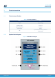
VL53L4CD Product overview 1 Product overview 1.1 Technical specification Table 1. Technical specification Feature Detail Package Optical LGA12 Size 4.4 x 2.4 x 1 mm Operating voltage 2.6 to 3.5 V Operating temperature -30 to 85°C Infrared emitter 940 nm I2C 1.2 Up to 1 MHz (Fast mode plus) serial bus Address: 0x52 System block diagram Figure 1.
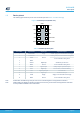
VL53L4CD Device pinout 1.3 Device pinout The following figure shows the pinout of the VL53L4CD (see also Section 6 Outline drawings). Figure 2. VL53L4CD pinout (bottom view) GND3 GPIO1 7 DNC 6 5 XSHUT 8 4 GND2 SDA 9 3 GND SCL 10 2 AVSSVCSEL AVDD 11 1 AVDDVCSEL 12 GND4 Table 2.
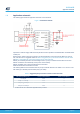
VL53L4CD Application schematic 1.4 Application schematic The following figure shows the application schematic of the VL53L4CD. Figure 3. VL53L4CD schematic Capacitors on external supply AVDD should be placed as close as possible to the AVDDVCSEL and AVSSVCSEL module pins. External pull up resistor values can be found in I2C-bus specification. Pull ups are typically fitted only once per bus, near the host. For suggested values see Table 3.
VL53L4CD Application schematic Table 4. Suggested pull up and series resistors for I2C Fast mode plus I2C load capacitance (CL)(1) Pull up resistor (Ohms) Series resistor (Ohms) CL ≤ 90 pF 1.5 k 100 90 pF < CL ≤ 140 pF 1k 50 140 pF < CL ≤ 270 pF 0.5 k 50 270 pF < CL ≤ 400 pF 0.3 k 50 1. For each bus line, CL is measured in application PCB by customer.
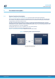
VL53L4CD Functional description 2 Functional description 2.1 System functional description Figure 4. VL53L4CD system functional description shows the system level functional description. The host customer application controls the VL53L4CD device using a driver called Ultra Lite Driver (ULD). The ULD contains a set of high level functions that allow control of the VL53L4CD Firmware (FW), like initialization, ranging start/stop, setting the system accuracy.
VL53L4CD State machine description 2.2 State machine description The following figure shows the device state machine. Figure 5. Device state machine 2.3 Customer manufacturing calibration flow Up to two calibrations are needed to ensure the best sensor performances. Offset needed in all applications. If a cover glass is used, cross-talk calibration is needed also. The detailed procedure is provided in the VL53L4CD Ultra Lite Driver user manual (UM2931). 2.
VL53L4CD Reading the results 2.6 Reading the results The software driver provides turnkey functions to read output results after the measurement: • Signal rate • Ranging distance • Measurement status A full description is provided in the VL53L4CD Ultra Lite Driver user manual (UM2931). 2.7 Power sequence There are two options available for device power up and boot sequence. Note: In all cases, XSHUT has to be raised only when AVDD is tied on.
VL53L4CD Ranging sequence 2.8 Ranging sequence Figure 8. Ranging sequence Note: API in the figure above means application programmable interface. Note: ttiming_budget is a parameter set by the user, using a dedicated driver function. 2.9 Handshake management Once a ranging measurement is available, an interrupt is generated. This is communicated to the host as a physical signal on the GPIO1 pin, which is driven low, and the output of a driver function.
VL53L4CD Control interface 3 Control interface This section specifies the control interface. The I2C interface uses two signals: serial data line (SDA) and serial clock line (SCL). Each device connected to the bus uses a unique address and a simple master / slave relationship exists. Both SDA and SCL lines are connected to a positive supply voltage using pull-up resistors located on the host. Lines are only actively driven low.
VL53L4CD Control interface Figure 11. Data format (write) As data are received by the slave, they are written bit by bit to a serial/parallel register. After each data byte has been received by the slave, an acknowledge is generated, the data are then stored in the internal register addressed by the current index. During a read message, the contents of the register addressed by the current index is read out in the byte following the device address byte.
VL53L4CD I2C interface - timing characteristics Figure 14. Data format (sequential read) 0x52 (write) ADDRESS[7:0] S INDEX[15:8] As INDEX[7:0] As As P 0x53 (read) S ADDRESS[7:0] DATA[7:0] 3.1 As Am DATA[7:0] DATA[7:0] Am Am DATA[7:0] DATA[7:0] Am Am P I2C interface - timing characteristics Timing characteristics are shown in the following tables. Refer to Figure 15. I2C timing characteristics for an explanation of the parameters used. Timings are given for all PVT conditions Table 5.
VL53L4CD I2C interface - timing characteristics Table 6. I2C interface - timing characteristics for Fast mode (400 kHz) Symbol Parameter Minimum Typical Maximum Unit FI2C Operating frequency 0 - 400 kHz tLOW Clock pulse width low 1.3 - - tHIGH Clock pulse width high 0.6 - - tSP Pulse width of spikes which are suppressed by the input filter - - 50 tBUF Bus free time between transmissions 1.3 - - tHD.STA Start hold time 0.26 - - tSU.STA Start setup time 0.26 - - tHD.
VL53L4CD I2C interface - reference registers 3.2 I2C interface - reference registers The registers shown in the table below can be used to validate the user I2C interface. Table 7. Reference registers Note: Register name Index Value Model_ID 0x010F 0xEB Module_Type 0x0110 0xAA The I2C read/writes can be 8,16 or 32-bit. Multi-byte reads/writes are always addressed in ascending order with MSB first as shown in the following table.
VL53L4CD Electrical characteristics 4 Electrical characteristics 4.1 Absolute maximum ratings Warning: Stresses above those listed in the following table may cause permanent damage to the device. This is a stress rating only and functional operation of the device at these or any other conditions above those indicated in the operational sections of the specification is not implied. Exposure to absolute maximum rating conditions for extended periods may affect device reliability. Table 9.
VL53L4CD Current consumption 4.4 Current consumption Table 12. Power consumption at ambient temperature All current consumption values include silicon process variations. Temperature and voltage are nominal conditions (23°C and 2v8). All values include AVDD and AVDDVCSEL. Parameter Min. Typ. Max. HW STANDBY 3 5 7 SW STANDBY 4 6 9 22 24 Active ranging average consumption (including VCSEL) (1) (2) Unit μA mA 1. Active ranging is an average value, measured using default driver settings. 2.
VL53L4CD Ranging performances 5 Ranging performances 5.1 Measurement conditions In all the measurement tables of this document, it is considered that: • All ranging performances are measured with the target covering the full FoV. • Charts used as targets are: gray (17% reflectance, N4.74 Munsell) and white (88% reflectance N9.5 Munsell). • Nominal voltage is 2.8 V and temperature is 23°C.
VL53L4CD Ranging accuracy 5.4 Ranging accuracy The figure below illustrates how range accuracy is defined over distance. Figure 16. Ranging accuracy vs. distance The ranging accuracy is a direct evaluation of the measurement error, including offset errors and output noise. At least 90% of the ranging values are within the declared ranges. This quality indicator includes measure-tomeasure and part-to-part dispersion. Table 15.
VL53L4CD Ranging drift with temperature 5.5 Ranging drift with temperature When the temperature increases, the ranging value may be affected. This value is an offset and not a gain, and it does not depend on the target distance. The device embeds a feature that allows to compensate the temperature variation effect. In order to get the most accurate performances, perform a manual temperature update when temperature varies. This operation is done using a dedicated driver function.
VL53L4CD Outline drawings 6 Outline drawings ST delivers any of the two alternative dual source cap assemblies as detailed in the drawings below. Both versions are transparent for the customer, since the pad and substrate design are identical for both versions and have no impact on customer PCB design. Ranging performances, reflow, and technical parameters are identical for all module designs presented in the figures below. Figure 17.
VL53L4CD Outline drawings Figure 18.
VL53L4CD Outline drawings Figure 19.
VL53L4CD Outline drawings Figure 20.
VL53L4CD Field of view (FoV) and field of illumination (FoI) 7 Field of view (FoV) and field of illumination (FoI) The Rx (or collector) exclusion zone includes all module assembly tolerances and is used to define the cover window dimensions. The cover window opening must be equal to or wider than the exclusion zone. The detection volume represents the applicative or system FoV in which a target is detected, and a distance measured.
VL53L4CD Laser safety considerations 8 Laser safety considerations The VL53L4CD contains a laser emitter and corresponding drive circuitry. The laser output is designed to remain within Class 1 laser safety limits under all reasonably foreseeable conditions including single faults in compliance with IEC 60825-1:2014 (third edition).
VL53L4CD Packaging and labeling 9 Packaging and labeling 9.1 Product marking A two line product marking is applied on the backside of the module (i.e. on the substrate). The first line is the silicon product code, and the second line, the internal tracking code. 9.2 Inner box labeling The labeling follows the ST standard packing acceptance specification. The following information will be on the inner box label: • Assembly site • Sales type • Quantity • Trace code • Marking • Bulk ID number 9.
VL53L4CD Tape outline drawing 9.4 Tape outline drawing Figure 24.
VL53L4CD Pb-free solder reflow process 9.5 Pb-free solder reflow process Table 17. Recommended solder profile and Figure 25. Solder profile show the recommended and maximum values for the solder profile. Customers have to tune the reflow profile depending on the PCB, solder paste and material used. We expect customers to follow the recommended reflow profile, which is specifically tuned for package.
VL53L4CD Handling and storage precautions 9.6 Handling and storage precautions 9.6.1 Shock precaution Sensor modules house numerous internal components that are susceptible to shock damage. If a unit is subject to excessive shock, is dropped on the floor, or a tray/reel of units is dropped on the floor, it must be rejected, even if no apparent damage is visible. 9.6.2 Part handling Handling must be done with non-marring ESD safe carbon, plastic, or teflon tweezers.
VL53L4CD Package information 10 Package information In order to meet environmental requirements, ST offers these devices in different grades of ECOPACK packages, depending on their level of environmental compliance. ECOPACK specifications, grade definitions and product status are available at: www.st.com. ECOPACK is an ST trademark.
VL53L4CD Ordering information 11 Ordering information Table 19.
VL53L4CD Revision history Table 20. Document revision history DS13812 - Rev 3 Date Version 15-Oct-2021 1 29-Oct-2021 2 03-Jan-2022 3 Changes Initial release Correct the Active Ranging values in Section 4.4 Current consumption Update Figure 16. Ranging accuracy vs.
VL53L4CD Contents Contents 1 2 3 4 5 Product overview . . . . . . . . . . . . . . . . . . . . . . . . . . . . . . . . . . . . . . . . . . . . . . . . . . . . . . . . . . . . . . . . . .3 1.1 Technical specification . . . . . . . . . . . . . . . . . . . . . . . . . . . . . . . . . . . . . . . . . . . . . . . . . . . . . . . . . . 3 1.2 System block diagram . . . . . . . . . . . . . . . . . . . . . . . . . . . . . . . . . . . . . . . . . . . . . . . . . . . . . . . . . . 3 1.3 Device pinout . . . .
VL53L4CD Contents 5.5 Ranging drift with temperature. . . . . . . . . . . . . . . . . . . . . . . . . . . . . . . . . . . . . . . . . . . . . . . . . . . 20 6 Outline drawings . . . . . . . . . . . . . . . . . . . . . . . . . . . . . . . . . . . . . . . . . . . . . . . . . . . . . . . . . . . . . . . . .21 7 Field of view (FoV) and field of illumination (FoI) . . . . . . . . . . . . . . . . . . . . . . . . . . . . . . . . . .25 8 Laser safety considerations. . . . . . . . . . . . . . . . . . . . . .
VL53L4CD IMPORTANT NOTICE – PLEASE READ CAREFULLY STMicroelectronics NV and its subsidiaries (“ST”) reserve the right to make changes, corrections, enhancements, modifications, and improvements to ST products and/or to this document at any time without notice. Purchasers should obtain the latest relevant information on ST products before placing orders. ST products are sold pursuant to ST’s terms and conditions of sale in place at the time of order acknowledgement.