
Datasheet

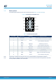

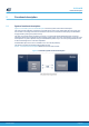


Table Of Contents
- Cover image
- Device summary
- Features
- Applications
- Description
- 1 Product overview
- 2 Functional description
- 3 Control interface
- 4 Electrical characteristics
- 5 Ranging performances
- 6 Outline drawings
- 7 Field of view (FoV) and field of illumination (FoI)
- 8 Laser safety considerations
- 9 Packaging and labeling
- 10 Package information
- 11 Ordering information
- Revision history
- Contents

1.3 Device pinout
The following figure shows the pinout of the VL53L4CD (see also Section 6 Outline drawings).
Figure 2. VL53L4CD pinout (bottom view)
AVDDVCSEL
2 AVSSVCSEL
3 GND
4 GND2
5 XSHUT
11 12AVDD
10SCL
9SDA
8DNC
7GPIO1 6
1
GND3
GND4
Table 2. VL53L4CD pin description
Pin number Signal name Signal type Signal description
1 AVDDVCSEL Supply VCSEL supply, to be connected to main supply
2 AVSSVCSEL
Ground
VCSEL ground, to be connected to main ground
3 GND
To be connected to main ground
4 GND2
5 XSHUT Digital input Xshutdown pin, active low
6 GND3 Ground To be connected to main ground
7 GPIO1 Digital output Interrupt output. Open drain output
8 DNC Digital input Do not connect, must be left floating
9 SDA Digital input/output I2C serial data
10 SCL Digital input I2C serial clock input
11 AVDD Supply Supply, to be connected to main supply
12 GND4 Ground To be connected to main ground
Note: AVSSVCSEL and GND are ground pins and can be connected together in the application schematics.
Note: GND2, GND3, and GND4 are standard pins that are forced to the ground domain in the application schematics
to avoid possible instabilities if set to other states.
VL53L4CD
Device pinout
DS13812 - Rev 3
page 4/36