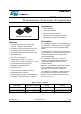
LSM9DS1 iNEMO inertial module: 3D accelerometer, 3D gyroscope, 3D magnetometer Datasheet - production data Applications Indoor navigation Smart user interfaces Advanced gesture recognition Gaming and virtual reality input devices LGA-24L (3.5x3x1.
Contents LSM9DS1 Contents 1 Pin description . . . . . . . . . . . . . . . . . . . . . . . . . . . . . . . . . . . . . . . . . . . . 10 2 Module specifications . . . . . . . . . . . . . . . . . . . . . . . . . . . . . . . . . . . . . . . 12 2.1 Sensor characteristics . . . . . . . . . . . . . . . . . . . . . . . . . . . . . . . . . . . . . . . 12 2.2 Electrical characteristics . . . . . . . . . . . . . . . . . . . . . . . . . . . . . . . . . . . . . . 13 2.2.1 3 4 2.
LSM9DS1 Contents 5.2 5.3 Accelerometer and gyroscope SPI bus interface . . . . . . . . . . . . . . . . . . . 31 5.2.1 SPI read . . . . . . . . . . . . . . . . . . . . . . . . . . . . . . . . . . . . . . . . . . . . . . . . . 32 5.2.2 SPI write . . . . . . . . . . . . . . . . . . . . . . . . . . . . . . . . . . . . . . . . . . . . . . . . 32 5.2.3 SPI read in 3-wire mode . . . . . . . . . . . . . . . . . . . . . . . . . . . . . . . . . . . . 33 Magnetic sensor SPI bus interface . . . . . . . . . .
Contents 8 4/72 LSM9DS1 7.23 CTRL_REG5_XL (1Fh) . . . . . . . . . . . . . . . . . . . . . . . . . . . . . . . . . . . . . . 51 7.24 CTRL_REG6_XL (20h) . . . . . . . . . . . . . . . . . . . . . . . . . . . . . . . . . . . . . . 51 7.25 CTRL_REG7_XL (21h) . . . . . . . . . . . . . . . . . . . . . . . . . . . . . . . . . . . . . . 52 7.26 CTRL_REG8 (22h) . . . . . . . . . . . . . . . . . . . . . . . . . . . . . . . . . . . . . . . . . . 53 7.27 CTRL_REG9 (23h) . . . . . . . . . . . . . . . . . . .
LSM9DS1 Contents 8.14 INT_CFG_M (30h) . . . . . . . . . . . . . . . . . . . . . . . . . . . . . . . . . . . . . . . . . . 67 8.15 INT_SRC_M (31h) . . . . . . . . . . . . . . . . . . . . . . . . . . . . . . . . . . . . . . . . . . 67 8.16 INT_THS_L(32h), INT_THS_H(33h) . . . . . . . . . . . . . . . . . . . . . . . . . . . . 68 9 Package information . . . . . . . . . . . . . . . . . . . . . . . . . . . . . . . . . . . . . . . . 69 10 Soldering information . . . . . . . . . . . . . . . . . . . . . .
List of tables LSM9DS1 List of tables Table 1. Table 2. Table 3. Table 4. Table 5. Table 6. Table 7. Table 8. Table 9. Table 10. Table 11. Table 12. Table 13. Table 14. Table 15. Table 16. Table 17. Table 18. Table 19. Table 20. Table 21. Table 22. Table 23. Table 24. Table 25. Table 26. Table 27. Table 28. Table 29. Table 30. Table 31. Table 32. Table 33. Table 34. Table 35. Table 36. Table 37. Table 38. Table 39. Table 40. Table 41. Table 42. Table 43. Table 44. Table 45. Table 46. Table 47. Table 48.
LSM9DS1 List of tables Table 49. Table 50. Table 51. Table 52. Table 53. Table 54. Table 55. Table 56. Table 57. Table 58. Table 59. Table 60. Table 61. Table 62. Table 63. Table 64. Table 65. Table 66. Table 67. Table 68. Table 69. Table 70. Table 71. Table 72. Table 73. Table 74. Table 75. Table 76. Table 77. Table 78. Table 79. Table 80. Table 81. Table 82. Table 83. Table 84. Table 85. Table 86. Table 87. Table 88. Table 89. Table 90. Table 91. Table 92. Table 93. Table 94. Table 95. Table 96.
List of tables Table 101. Table 102. Table 103. Table 104. Table 105. Table 106. Table 107. Table 108. Table 109. Table 110. Table 111. Table 112. Table 113. Table 114. Table 115. Table 116. Table 117. Table 118. Table 119. Table 120. Table 121. Table 122. Table 123. Table 124. Table 125. Table 126. Table 127. Table 128. Table 129. Table 130. Table 131. Table 132. 8/72 LSM9DS1 OFFSET_X_REG_L_M register . . . . . . . . . . . . . . . . . . . . . . . . . . . . . . . . . . . . . . . . . . . . .
LSM9DS1 List of figures List of figures Figure 1. Figure 2. Figure 3. Figure 4. Figure 5. Figure 6. Figure 7. Figure 8. Figure 9. Figure 10. Figure 11. Figure 12. Figure 13. Figure 14. Figure 15. Figure 16. Figure 17. Figure 18. Figure 19. Figure 20. Figure 21. Figure 22. Figure 23. Figure 24. Figure 25. Figure 26. Figure 27. Figure 28. Figure 29. Figure 30. Figure 31. Pin connections . . . . . . . . . . . . . . . . . . . . . . . . . . . . . . . . . . . . . . . . . . . . . . . . . . . . . . . . .
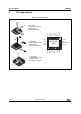
Pin description 1 LSM9DS1 Pin description Figure 1.
LSM9DS1 Pin description Table 2.
Module specifications LSM9DS1 2 Module specifications 2.1 Sensor characteristics @ Vdd = 2.2 V, T = 25 °C unless otherwise noted(a) Table 3. Sensor characteristics Symbol Parameter Test conditions Min. Typ.(1) Max.
LSM9DS1 2.2 Module specifications Electrical characteristics @ Vdd = 2.2 V, T = 25 °C unless otherwise noted(b) Table 4. Electrical characteristics Symbol Vdd Test conditions Parameter Min. Typ.(1) Max. Unit V Supply voltage 1.9 3.6 Vdd_IO Module power supply for I/O 1.71 Vdd+0.1 Idd_XM Current consumption of the accelerometer and magnetic sensor in normal mode (2) 600 μA Gyroscope current consumption in normal mode(3) 4.
Module specifications 2.2.1 LSM9DS1 Recommended power-up sequence For the power-up sequence please refer to the following figure, where: Trise is the time for the power supply to rise from 10% to 90% of its final value Twait is the delay between the end of the Vdd_IO ramp (90% of its final value) and the start of the Vdd ramp Figure 2. Recommended power-up sequence Trise Vdd_IO 0V Twait Vdd 0V Trise 2.3 Temperature sensor characteristics @ Vdd = 2.
LSM9DS1 Module specifications 2.4 Communication interface characteristics 2.4.1 SPI - serial peripheral interface Subject to general operating conditions for Vdd and Top. Table 6.
Module specifications 2.4.2 LSM9DS1 I2C - inter-IC control interface Subject to general operating conditions for Vdd and Top. Table 7. I2C slave timing values Symbol f(SCL) I2C Standard mode(1) Parameter SCL clock frequency I2C Fast mode (1) Min Max Min Max 0 100 0 400 tw(SCLL) SCL clock low time 4.7 1.3 tw(SCLH) SCL clock high time 4.0 0.6 tsu(SDA) SDA setup time 250 100 th(SDA) SDA data hold time 0 th(ST) START condition hold time 4 0.
LSM9DS1 2.5 Module specifications Absolute maximum ratings Stresses above those listed as “Absolute maximum ratings” may cause permanent damage to the device. This is a stress rating only and functional operation of the device under these conditions is not implied. Exposure to maximum rating conditions for extended periods may affect device reliability. Table 8. Absolute maximum ratings Symbol Vdd Vdd_IO Vin Note: Ratings Maximum value Unit Supply voltage -0.3 to 4.
Module specifications 2.6 Terminology 2.6.1 Sensitivity LSM9DS1 Linear acceleration sensitivity can be determined, for example, by applying 1 g acceleration to the device. Because the sensor can measure DC accelerations, this can be done easily by pointing the selected axis towards the ground, noting the output value, rotating the sensor 180 degrees (pointing towards the sky) and noting the output value again. By doing so, ±1 g acceleration is applied to the sensor.
LSM9DS1 LSM9DS1 functionality 3 LSM9DS1 functionality 3.1 Operating modes In the LSM9DS1 the accelerometer and gyroscope have two operating modes available: only accelerometer active and gyroscope in power down or both accelerometer and gyroscope sensors active at the same ODR.
LSM9DS1 functionality LSM9DS1 Table 9. Gyroscope operating modes ODR_G [2:0] ODR [Hz] Power mode 000 Power down Power-down 001 14.9 Low-power/Normal mode 010 59.5 Low-power/Normal mode 011 119 Low-power/Normal mode 100 238 Normal mode 101 476 Normal mode 110 952 Normal mode Table 10. Operating mode current consumption ODR [Hz] Current consumption(1) Power mode [mA] 14.9 Low-power 1.9 59.5 Low-power 2.4 119 Low-power 3.1 238 Normal mode 4.3 476 Normal mode 4.
LSM9DS1 LSM9DS1 functionality Table 12. Gyroscope turn-on time LPF1 only(1) ODR [Hz] LPF1 and LPF2(1) 14.9 2 LPF2 not available 59.5 or 119 3 13 238 4 14 476 5 15 952 8 18 1. The table contains the number of samples to be discarded after switching between low-power mode and normal mode. 3.3 Accelerometer and gyroscope multiple reads (burst) When only accelerometer is activated and the gyroscope is in power down, starting from OUT_X_XL (28h - 29h) multiple reads can be performed.
LSM9DS1 functionality 3.4 LSM9DS1 Block diagram Figure 8. Accelerometer and gyroscope digital block diagram HR HPIS1 0 0 LPF2 XL Interrupt Generator XL 1 1 ADC XL LPF1 XL HPF XL 0 1 FDS OUT_SEL Data Reg FIFO 0 ADC Gyro LPF1 Gyro 1 HPF Gyro I2C / SPI (XL + Gyro) LPF2 Gyro SRC Registers CFG Registers HP_EN Interrupt Generator Gyro INT_SEL Figure 9.
LSM9DS1 3.5 LSM9DS1 functionality Accelerometer and gyroscope FIFO The LSM9DS1 embeds 32 slots of 16-bit data FIFO for each of the gyroscope’s three output channels, yaw, pitch and roll, and 16-bit data FIFO for each of the accelerometer’s three output channels, X, Y and Z. This allows consistent power saving for the system since the host processor does not need to continuously poll data from the sensor, but it can wake up only when needed and burst the significant data out from the FIFO.
LSM9DS1 functionality 3.5.2 LSM9DS1 FIFO mode In FIFO mode (FIFO_CTRL (2Eh) (FMODE [2:0] = 001) data from the output channels are stored in the FIFO until it is overwritten. To reset FIFO content, Bypass mode should be selected by writing FIFO_CTRL (2Eh) (FMODE [2:0]) to '000'. After this reset command, it is possible to restart FIFO mode by writing FIFO_CTRL (2Eh) (FMODE [2:0]) to '001'.
LSM9DS1 LSM9DS1 functionality Figure 12. Continuous mode xi,yi,zi 3.5.4 x0 y0 z0 x1 y1 z1 x2 y2 z2 x30 y30 z30 x31 y31 z31 Continuous-to-FIFO mode In Continuous-to-FIFO mode (FIFO_CTRL (2Eh)(FMODE [2:0] = 011), FIFO behavior changes according to the INT_GEN_SRC_XL (26h)(IA_XL) bit. When the INT_GEN_SRC_XL (26h)(IA_XL) bit is equal to '1', FIFO operates in FIFO-mode, when the INT_GEN_SRC_XL (26h)(IA_XL) bit is equal to '0', FIFO operates in Continuous mode.
LSM9DS1 functionality 3.5.5 LSM9DS1 Bypass-to-Continuous mode In Bypass-to-Continuous mode (FIFO_CTRL (2Eh)(FMODE[2:0] = '100'), data measurement storage inside FIFO operates in Continuous mode when INT_GEN_SRC_XL (26h)(IA_XL) is equal to '1', otherwise FIFO content is reset (Bypass mode). The interrupt generator should be set to the desired configuration by means of INT_GEN_CFG_XL (06h), INT_GEN_THS_X_XL (07h), INT_GEN_THS_Y_XL (08h) and INT_GEN_THS_Z_XL (09h).
LSM9DS1 Application hints 4 Application hints Figure 15. LSM9DS1 electrical connections Vdd C3 C4 100 nF GND 10 μF GND *C5 10nF(16V) C1 Vdd_IO 100 nF GND GND C2 RES GND GND CAP VDD VDD C1 VDD_IO 100 nF GND 18 1 RES SCL/SPC VDD_IO RES (TOP VIEW) RES SDA/SDI/SDO RES SDO_A/G 6 13 DEN_A/G INT1_A/G INT2_A/G INT_M CS_M DRDY_M SDO_M CS_A/G GND * C5 must guarantee 1 nF value under 11 V bias condition 4.1 External capacitors The device core is supplied through the Vdd line.
Digital interfaces 5 LSM9DS1 Digital interfaces The registers embedded inside the LSM9DS1 may be accessed through both the I2C and SPI serial interfaces. The latter may be SW configured to operate either in 3-wire or 4-wire interface mode. The serial interfaces are mapped onto the same pins. To select/exploit the I2C interface, the CS line must be tied high (i.e connected to Vdd_IO). Table 13.
LSM9DS1 Digital interfaces I2C operation 5.1.1 The transaction on the bus is started through a START (ST) signal. A START condition is defined as a high-to-low transition on the data line while the SCL line is held high. After this has been transmitted by the master, the bus is considered busy.
Digital interfaces LSM9DS1 some other function, it can hold the clock line, SCL low to force the transmitter into a wait state. Data transfer only continues when the receiver is ready for another byte and releases the data line. If a slave receiver doesn’t acknowledge the slave address (i.e. it is not able to receive because it is performing some real-time function) the data line must be left high by the slave. The master can then abort the transfer.
LSM9DS1 5.2 Digital interfaces Accelerometer and gyroscope SPI bus interface The LSM9DS1 accelerometer and gyroscope SPI is a bus slave. The SPI allows to write and read the registers of the device. The Serial Interface connects to applications using 4 wires: CS_A/G, SPC, SDI and SDO_A/G. Figure 16.
Digital interfaces 5.2.1 LSM9DS1 SPI read Figure 17. Accelerometer and gyroscope SPI read protocol CS_A/G CS SPC SDI RW AD6 AD5 AD4 AD3 AD2 AD1 AD0 SDO_A/G SDO DO7 DO6 DO5 DO4 DO3 DO2 DO1 DO0 The SPI read command is performed with 16 clock pulses. A multiple byte read command is performed by adding blocks of 8 clock pulses to the previous one. bit 0: READ bit. The value is 1. bit 1-7: address AD(6:0). This is the address field of the indexed register. bit 8-15: data DO(7:0) (read mode).
LSM9DS1 Digital interfaces bit 8-15: data DI(7:0) (write mode). This is the data that is written inside the device (MSb first). bit 16-... : data DI(...-8). Further data in multiple byte writes. Figure 20. Multiple byte SPI write protocol (2-byte example) CS_A/G CS SPC SDI DI7 DI6 DI5 DI4 DI3 DI2 DI1 DI0 DI15 DI14 DI13 DI12 DI11 DI10 DI9 DI8 RW AD6 AD5 AD4 AD3 AD2 AD1 AD0 5.2.
Digital interfaces 5.3 LSM9DS1 Magnetic sensor SPI bus interface The LSM9DS1 magnetic sensor SPI is a bus slave. The SPI allows writing and reading the registers of the device. The serial interface connects to applications using 4 wires: CS_M, SPC, SDI and SDO_M. Figure 22.
LSM9DS1 5.3.1 Digital interfaces SPI read Figure 23. Magnetic sensor SPI read protocol CS_M CS SPC SDI RW MS AD5 AD4 AD3 AD2 AD1 AD0 SDO_M SDO DO7 DO6 DO5 DO4 DO3 DO2 DO1 DO0 AM10130V1 The SPI read command is performed with 16 clock pulses. A multiple byte read command is performed by adding blocks of 8 clock pulses to the previous one. bit 0: READ bit. The value is 1. bit 1: MS bit. When 0, does not increment the address; when 1, increments the address in multiple reads. bit 2-7: address AD(5:0).
Digital interfaces 5.3.2 LSM9DS1 SPI write Figure 25. Magnetic sensor SPI write protocol CS_M CS SPC SDI D I7 D I6 D I5 D I4 DI3 DI2 DI1 DI0 RW MS AD5 AD 4 AD 3 AD2 AD 1 AD0 AM10132V1 The SPI write command is performed with 16 clock pulses. A multiple byte write command is performed by adding blocks of 8 clock pulses to the previous one. bit 0: WRITE bit. The value is 0. bit 1: MS bit. When 0, does not increment the address; when 1, increments the address in multiple writes.
LSM9DS1 5.3.3 Digital interfaces SPI read in 3-wire mode 3-wire mode is entered by setting the SIM bit to ‘1’ (SPI serial interface mode selection) in CTRL_REG3_M (22h). When 3-wire mode is used, the SDO_M pin has to be connected to GND or Vdd_IO. Figure 27. SPI read protocol in 3-wire mode CS_M CS SPC SDI/O D O7 D O6 D O5 DO4 DO3 DO2 DO1 DO0 RW MS AD5 AD 4 AD 3 AD2 AD1 AD 0 AM10134V1 The SPI read command is performed with 16 clock pulses: bit 0: READ bit. The value is 1. bit 1: MS bit.
Register mapping 6 LSM9DS1 Register mapping The table given below provides a list of the 8/16-bit registers embedded in the device and the corresponding addresses. Table 21.
LSM9DS1 Register mapping Table 21.
Register mapping LSM9DS1 Table 22.
LSM9DS1 7 Accelerometer and gyroscope register description Accelerometer and gyroscope register description The device contains a set of registers which are used to control its behavior and to retrieve linear acceleration, angular rate and temperature data. The register addresses, made up of 7 bits, are used to identify them and to write the data through the serial interface. 7.1 ACT_THS (04h) Activity threshold register. Table 23.
Accelerometer and gyroscope register description LSM9DS1 Table 28. INT_GEN_CFG_XL register description AOI_XL AND/OR combination of accelerometer’s interrupt events. Default value: 0 (0: OR combination; 1: AND combination) 6D 6-direction detection function for interrupt. Default value: 0 (0: disabled; 1: enabled) ZHIE_XL Enable interrupt generation on accelerometer’s Z-axis high event.
LSM9DS1 7.6 Accelerometer and gyroscope register description INT_GEN_THS_Z_XL (09h) Linear acceleration sensor interrupt threshold register. Table 33. INT_GEN_THS_Z_XL register THS_XL_Z THS_XL_Z THS_XL_Z THS_XL_Z THS_XL_Z THS_XL_Z THS_XL_Z THS_XL_Z 7 6 5 4 3 2 1 0 Table 34. INT_GEN_THS_Z_XL register description THS_XL_Z [7:0] 7.7 Z-axis interrupt threshold. Default value: 0000 0000 INT_GEN_DUR_XL (0Ah) Linear acceleration sensor interrupt duration register. Table 35.
Accelerometer and gyroscope register description LSM9DS1 Table 40. INT1_CTRL register description Gyroscope interrupt enable on INT 1_A/G pin. Default value: 0 INT1_IG_G (0: disabled; 1: enabled) Accelerometer interrupt generator on INT 1_A/G pin. Default value: 0 INT_ IG_XL (0: disabled; 1: enabled) FSS5 interrupt enable on INT 1_A/G pin. Default value: 0 INT_ FSS5 (0: disabled; 1: enabled) Overrun interrupt on INT 1_A/G pin.
LSM9DS1 7.11 Accelerometer and gyroscope register description WHO_AM_I (0Fh) Who_AM_I register. Table 43. WHO_AM_I register 0 7.12 1 1 0 1 0 0 0 BW_G1 BW_G0 CTRL_REG1_G (10h) Angular rate sensor Control Register 1. Table 44. CTRL_REG1_G register ODR_G2 ODR_G1 ODR_G0 FS_G1 FS_G0 0(1) 1. This bit must be set to ‘0’ for the correct operation of the device. Table 45. CTRL_REG1_G register description Gyroscope output data rate selection.
Accelerometer and gyroscope register description LSM9DS1 Table 47. ODR and BW configuration setting (after LPF2) ODR_G [2:0] BW_G [1:0] Cutoff [Hz](1) ODR [Hz] 000 00 Power-down n.a. 000 01 Power-down n.a. 000 10 Power-down n.a. 000 11 Power-down n.a. 001 00 14.9 n.a. 001 01 14.9 n.a. 001 10 14.9 n.a. 001 11 14.9 n.a. 010 00 59.5 16 010 01 59.5 16 010 10 59.5 16 010 11 59.
LSM9DS1 7.13 Accelerometer and gyroscope register description CTRL_REG2_G (11h) Angular rate sensor Control Register 2. Table 48. CTRL_REG2_G register 0 (1) 0 (1) 0(1) 0(1) INT_SEL1 INT_SEL0 OUT_SEL1 OUT_SEL0 1. These bits must be set to ‘0’ for the correct operation of the device Table 49. CTRL_REG2_G register description INT_SEL [1:0] INT selection configuration. Default value: 00 (Refer to Figure 28) OUT_SEL [1:0] Out selection configuration.
Accelerometer and gyroscope register description LSM9DS1 Table 52. Gyroscope high-pass filter cutoff frequency configuration [Hz](1) ODR= 14.9 ODR= 59.5 Hz Hz ODR= 119 Hz ODR= 238 Hz ODR= 476 Hz ODR= 952 Hz 0000 1 4 8 15 30 57 0001 0.5 2 4 8 15 30 0010 0.2 1 2 4 8 15 0011 0.1 0.5 1 2 4 8 0100 0.05 0.2 0.5 1 2 4 0101 0.02 0.1 0.2 0.5 1 2 0110 0.01 0.05 0.1 0.2 0.5 1 0111 0.005 0.02 0.05 0.1 0.2 0.5 1000 0.002 0.01 0.02 0.05 0.1 0.
LSM9DS1 Accelerometer and gyroscope register description Table 56. INT_GEN_SRC_G register description 7.17 IA_G Interrupt active. Default value: 0 (0: no interrupt has been generated; 1: one or more interrupts have been generated) ZH_G Yaw (Z) high. Default value: 0 (0: no interrupt, 1: Z high event has occurred) ZL_G Yaw (Z) low. Default value: 0 (0: no interrupt; 1: Z low event has occurred) YH_G Roll (Y) high. Default value: 0 (0: no interrupt, 1: Y high event has occurred) YL_G Roll (Y) low.
Accelerometer and gyroscope register description LSM9DS1 Table 61. STATUS_REG register description 7.19 IG_XL Accelerometer interrupt output signal. Default value: 0 (0: no interrupt has been generated; 1: one or more interrupt events have been generated) IG_G Gyroscope interrupt output signal. Default value: 0 (0: no interrupt has been generated; 1: one or more interrupt events have been generated) INACT Inactivity interrupt output signal.
LSM9DS1 Accelerometer and gyroscope register description Table 63. CTRL_REG4 register description 7.23 Zen_G Gyroscope’s Yaw axis (Z) output enable. Default value: 1 (0: Z-axis output disabled; 1: Z-axis output enabled) Yen_G Gyroscope’s roll axis (Y) output enable. Default value: 1 (0: Y-axis output disabled; 1: Y-axis output enabled) Xen_G Gyroscope’s pitch axis (X) output enable. Default value: 1 (0: X -xis output disabled; 1: X-axis output enabled) LIR_XL1 Latched Interrupt.
Accelerometer and gyroscope register description LSM9DS1 Table 67. CTRL_REG6_XL register description ODR_XL [2:0] Output data rate and power mode selection. default value: 000 (see Table 68) FS_XL [1:0] Accelerometer full-scale selection. Default value: 00 (00: ±2g; 01: ±16 g; 10: ±4 g; 11: ±8 g) BW_SCAL_ ODR Bandwidth selection.
LSM9DS1 Accelerometer and gyroscope register description Table 70. CTRL_REG7_XL register description High resolution mode for accelerometer enable. Default value: 0 (0: disabled; 1: enabled). Refer to Table 71 HR DCF[1:0] FDS Accelerometer digital filter (high pass and low pass) cutoff frequency selection: the bandwidth of the high-pass filter depends on the selected ODR. Refer to Table 71 Filtered data selection.
Accelerometer and gyroscope register description 7.27 LSM9DS1 CTRL_REG9 (23h) Control register 9. Table 74. CTRL_REG9 register 0(1) SLEEP_G FIFO_ TEMP_EN 0(1) DRDY_ mask_bit I2C_DISAB STOP_ON FIFO_EN LE _FTH 1. These bits must be set to ‘0’ for the correct operation of the device Table 75. CTRL_REG9 register description SLEEP_G Gyroscope sleep mode enable. Default value: 0 (0: disabled; 1: enabled) FIFO_TEMP_EN Temperature data storage in FIFO enable.
LSM9DS1 Accelerometer and gyroscope register description Table 79. INT_GEN_SRC_XL register description 7.30 IA_XL Interrupt active. Default value: 0. (0: no interrupt has been generated; 1: one or more interrupts have been generated) ZH_XL Accelerometer’s Z high event. Default value: 0 (0: no interrupt, 1: Z high event has occurred) ZL_XL Accelerometer’s Z low event. Default value: 0 (0: no interrupt; 1: Z low event has occurred) YH_XL Accelerometer’s Y high event.
Accelerometer and gyroscope register description 7.31 LSM9DS1 OUT_X_XL (28h - 29h) Linear acceleration sensor X-axis output register. The value is expressed as a 16-bit word in two’s complement. 7.32 OUT_Y_XL (2Ah - 2Bh) Linear acceleration sensor Y-axis output register. The value is expressed as a 16-bit word in two’s complement. 7.33 OUT_Z_XL (2Ch - 2Dh) Linear acceleration sensor Z-axis output register. The value is expressed as a 16-bit word in two’s complement. 7.
LSM9DS1 7.35 Accelerometer and gyroscope register description FIFO_SRC (2Fh) FIFO status control register. Table 85. FIFO_SRC register FTH OVRN FSS5 FSS4 FSS3 FSS2 FSS1 FSS0 Table 86. FIFO_SRC register description FTH FIFO threshold status. (0: FIFO filling is lower than threshold level; 1: FIFO filling is equal or higher than threshold level OVRN FIFO overrun status.
Accelerometer and gyroscope register description LSM9DS1 Table 89. INT_GEN_CFG_G register description 7.37 AOI_G AND/OR combination of gyroscope’s interrupt events. Default value: 0 (0: OR combination; 1: AND combination) LIR_G Latch Gyroscope interrupt request. Default value: 0. (0: interrupt request not latched; 1: interrupt request latched) ZHIE_G Enable interrupt generation on gyroscope’s yaw (Z) axis high event.
LSM9DS1 7.38 Accelerometer and gyroscope register description INT_GEN_THS_Y_G (33h - 34h) Angular rate sensor interrupt generator threshold registers. The value is expressed as a 15-bit word in two’s complement. Table 93. INT_GEN_THS_YH_G register 0(1) THS_G_ Y14 THS_G_ Y13 THS_G_ Y12 THS_G_ Y11 THS_G_ Y10 THS_G_ Y9 THS_G_ Y8 THS_G_ Y1 THS_G_ Y0 1. This bit must be set to ‘0’ for the correct operation of the device. Table 94.
Accelerometer and gyroscope register description LSM9DS1 Table 100. INT_GEN_DUR_G register description WAIT_G Exit from interrupt wait function enable. Default value: 0 (0: wait function off; 1: wait for DUR_G [6:0] samples before exiting interrupt) DUR_G [6:0] Enter/exit interrupt duration value. Default Value: 000 0000 The DUR_G [6:0] bits set the minimum duration of the interrupt event to be recognized. Duration steps and maximum values depend on the ODR chosen.
LSM9DS1 Accelerometer and gyroscope register description Figure 30.
Magnetometer register description LSM9DS1 8 Magnetometer register description 8.1 OFFSET_X_REG_L_M (05h), OFFSET_X_REG_H_M (06h) This register is a 16-bit register and represents the X offset used to compensate environmental effects (data is expressed as two’s complement). This value acts on the magnetic output data value in order to subtract the environmental offset. Default value: 0 Table 101.
LSM9DS1 8.4 Magnetometer register description WHO_AM_I_M (0Fh) Device identification register. Table 107. WHO_AM_I_M register 0 8.5 0 1 1 1 1 0 1 0(1) ST CTRL_REG1_M (20h) Table 108. CTRL_REG1_M register TEMP_ COMP OM1 OM0 DO2 DO1 DO0 1. This bit must be set to ‘0’ for the correct operation of the device Table 109. CTRL_REG1_M register description TEMP_COMP Temperature compensation enable.
Magnetometer register description 8.6 LSM9DS1 CTRL_REG2_M (21h) Table 112. CTRL_REG2_M register 0 (1) FS1 FS0 0(1) REBOOT SOFT_RST 0(1) 0(1) 1. These bits must be set to ‘0’ for the correct operation of the device. Table 113. CTRL_REG2_M register description FS[1:0] Full-scale configuration. Default value: 00 Refer to Table 114 REBOOT Reboot memory content. Default value: 0 (0: normal mode; 1: reboot memory content) SOFT_RST Configuration registers and user register reset function.
LSM9DS1 Magnetometer register description Table 117. System operating mode selection 8.8 MD1 MD0 Mode 0 0 Continuous-conversion mode 0 1 Single-conversion mode 1 0 Power-down mode 1 1 Power-down mode CTRL_REG4_M (23h) Table 118. CTRL_REG4_M register 0(1) 0(1) 0(1) 0(1) OMZ1 OMZ0 BLE 0(1) 1. These bits must be set to ‘0’ for the correct operation of the device Table 119. CTRL_REG4_M register description OMZ[1:0] Z-axis operative mode selection. Default value: 00.
Magnetometer register description 8.10 LSM9DS1 STATUS_REG_M (27h) Table 123. STATUS_REG_M register ZYXOR ZOR YOR XOR ZYXDA ZDA ZYXOR X, Y and Z-axis data overrun. Default value: 0 (0: no overrun has occurred; 1: a new set of data has overwritten the previous set) ZOR Z-axis data overrun. Default value: 0 (0: no overrun has occurred; 1: new data for the Z-axis has overwritten the previous data) YOR Y-axis data overrun.
LSM9DS1 8.14 Magnetometer register description INT_CFG_M (30h) Table 125. INT_CFG_M register XIEN YIEN 0(1) ZIEN 0(1) IEA IEL IEN 1. This bit must be set to ‘0’ for the correct operation of the device. Table 126. INT_CFG_M register description 8.15 XIEN Enable interrupt generation on X-axis. Default value: 0 0: disable interrupt request; 1: enable interrupt request YIEN Enable interrupt generation on Y-axis.
Magnetometer register description 8.16 LSM9DS1 INT_THS_L(32h), INT_THS_H(33h) Interrupt threshold. Default value: 0. The value is expressed in 15-bit unsigned. Even if the threshold is expressed in absolute value, the device detects both positive and negative thresholds. Table 129. INT_THS_L_M register THS7 THS6 THS5 THS4 THS3 THS2 THS1 THS0 THS9 THS8 Table 130. INT_THS_H_M register 0(1) THS14 THS13 THS12 THS11 1. This bit must be set to ‘0’ for the correct operation of the device.
LSM9DS1 9 Package information Package information In order to meet environmental requirements, ST offers these devices in different grades of ECOPACK® packages, depending on their level of environmental compliance. ECOPACK® specifications, grade definitions and product status are available at: www.st.com. ECOPACK is an ST trademark. Table 131. LGA (3.5x3x1 mm) 24-lead mechanical data mm Dim. Min. Typ. Max. A1 1.000 1.027 A3 0.130 D1 2.850 3.000 3.150 E1 3.350 3.500 3.650 L1 2.960 3.
Soldering information 10 LSM9DS1 Soldering information The LGA package is compliant with the ECOPACK®, RoHS and “Green” standard. It is qualified for soldering heat resistance according to JEDEC J-STD-020. Leave “Pin 1 Indicator” unconnected during soldering. Land pattern and soldering recommendations are available at www.st.com/mems.
LSM9DS1 11 Revision history Revision history Table 132. Document revision history Date Revision 18-Dec-2013 1 Initial release 2 Datasheet status promoted from preliminary to production data Added ±16 g linear acceleration full scale throughout datasheet Corrected typo in footnote 3, 4 and 5 of Table 2: Pin description Updated Figure 15: LSM9DS1 electrical connections and Section 4.
LSM9DS1 IMPORTANT NOTICE – PLEASE READ CAREFULLY STMicroelectronics NV and its subsidiaries (“ST”) reserve the right to make changes, corrections, enhancements, modifications, and improvements to ST products and/or to this document at any time without notice. Purchasers should obtain the latest relevant information on ST products before placing orders. ST products are sold pursuant to ST’s terms and conditions of sale in place at the time of order acknowledgement.