
Data Sheet


SD7
SC7
SD6
SC6
SC4
SD4
SD0
A0
A1
RESET
SC0
SD1
SC1
GND
VCC
SDA
SCL
A2
SD3
SC3
SD2
SC2
V
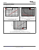
DPU0
Via to Power Plane
Partial Power Plane
V
DPUM
Via to GND Plane
Copper Pour
V
CC
GND
By-pass/de-coupling
capacitors
TCA9548A
GND
To I
2
C Master
To Slave Channel 0
LEGEND
SC5
SD5
(inner layer)
(outer layer)
V
DPU2
To Slave Channel 2
V
DPU1
To Slave Channel 1
V
DPU6
To Slave Channel 6
V
DPU5
To Slave Channel 5
V
DPU3
To Slave Channel 3
V
DPU4
To Slave Channel 4
V
DPU7
To Slave Channel 7
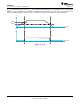
1
2
3
4
5
6
7
8
9
10
11
12 13
14
15
16
17
18
19
20
21
22
23
24
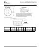
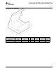
PW package
25
TCA9548A
www.ti.com
SCPS207F –MAY 2012–REVISED NOVEMBER 2016
Product Folder Links: TCA9548A
Submit Documentation FeedbackCopyright © 2012–2016, Texas Instruments Incorporated
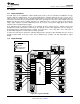
11 Layout
11.1 Layout Guidelines
For PCB layout of the TCA9548A, common PCB layout practices must be followed but additional concerns
related to high-speed data transfer such as matched impedances and differential pairs are not a concern for I
2
C
signal speeds. It is common to have a dedicated ground plane on an inner layer of the board and pins that are
connected to ground must have a low-impedance path to the ground plane in the form of wide polygon pours and
multiple vias. By-pass and de-coupling capacitors are commonly used to control the voltage on the VCC pin,
using a larger capacitor to provide additional power in the event of a short power supply glitch and a smaller
capacitor to filter out high-frequency ripple.
In an application where voltage translation is not required, all V
DPUX
voltages and V
CC
could be at the same
potential and a single copper plane could connect all of pull-up resistors to the appropriate reference voltage. In
an application where voltage translation is required, V
DPUM
and V
DPU0
– V
DPU7
, may all be on the same layer of
the board with split planes to isolate different voltage potentials.
To reduce the total I
2
C bus capacitance added by PCB parasitics, data lines (SCn and SDn) must be a short as
possible and the widths of the traces must also be minimized (for example, 5-10 mils depending on copper
weight).
11.2 Layout Example
Figure 20. Layout Schematic