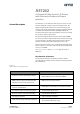
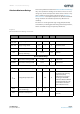
AS7262 6-Channel Visible Spectral_ID Device with Electronic Shutter and Smart Interface General Description The AS7262 is a cost-effective multi-spectral sensor-on-chip solution designed to address spectral ID applications. This highly integrated device delivers 6-channel multi-spectral sensing in the visible wavelengths from approximately 430nm to 670nm with full-width half-max (FWHM) of 40nm. An integrated LED driver with programmable current is provided for electronic shutter applications.
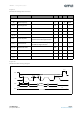
AS7262 − General Description Applications The AS7262 applications include: • Portable spectrometry • Horticulture • Color matching and identification • Authentication and brand protection • Precision color tuning/calibration Block Diagram The system blocks of this device are shown below.
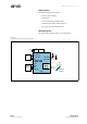
AS7262 − Pin Assignments Pin Assignments The device pin assignments are described below.
AS7262 − Pin Assignments Pin Number Pin Name 15 LED_DRV 16 GND Ground 17 VDD1 Voltage Supply 18 LED_IND 19 NF Not Functional. Do not connect. 20 NF Not Functional. Do not connect.
AS7262 − Absolute Maximum Ratings Absolute Maximum Ratings Stresses beyond those listed under Absolute Maximum Ratings may cause permanent damage to the device. These are stress ratings only. Functional operation of the device at these or any other conditions beyond those indicated under Electrical Characteristics is not implied. Exposure to absolute maximum rating conditions for extended periods may affect device reliability.
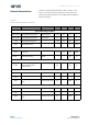
AS7262 − Electrical Characteristics Electrical Characteristics All limits are guaranteed with VDD = VDD1 = VDD2 = 3.3V, TAMB = 25°C. The parameters with min and max values are guaranteed with production tests or SQC (Statistical Quality Control) methods. Figure 6: Electrical Characteristics of AS7262 Symbol Parameter Conditions Min Typ Max Unit General Operating Conditions VDD1 /VDD2 Voltage Operating Supply UART Interface 2.97 3.3 3.
AS7262 − Electrical Characteristics Symbol Parameter Conditions Min Typ Max Unit Digital Inputs and Outputs IIH, IIL Logic Input Current Vin=0V or VDD -1 1 μA IIL RESN Logic Input Current (RESN pin) Vin=0V -1 -0.2 mA VIH CMOS Logic High Input 0.7* VDD VDD V VIL CMOS Logic Low Input 0 0.3* VDD V VOH CMOS Logic High Output I=1mA VDD-0.4 V VOL CMOS Logic Low Output I=1mA 0.
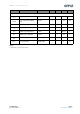
AS7262 − Timing Characteristics Timing Characteristics Figure 7: AS7262 I²C Slave Timing Characteristics Symbol Parameter Conditions Min Typ Max Unit 400 kHz I²C Interface fSCLK SCL Clock Frequency tBUF Bus Free Time Between a STOP and START 1.3 μs Hold Time (Repeated) START 0.6 μs tLOW LOW Period of SCL Clock 1.3 μs tHIGH HIGH Period of SCL Clock 0.6 μs tSU:STA Setup Time for a Repeated START 0.
AS7262 − Timing Characteristics Figure 9: AS7262 SPI Timing Characteristics Symbol Parameter Conditions Min Typ Max Unit 16 MHz SPI Interface fSCK Clock Frequency 0 tSCK_H Clock High Time 40 ns tSCK_L Clock Low Time 40 ns tSCK_RISE SCK Rise Time 5 ns tSCK_FALL SCK Fall Time 5 ns tCSN_S CSN Setup Time Time between CSN high-low transition to first SCK high transition 50 ns tCSN_H CSN Hold Time Time between last SCK falling edge and CSN low-high transition 100 ns tCSN_DI
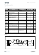
AS7262 − Timing Characteristics Figure 11: SPI Master Read Timing Diagram CSN_xx tSCK _H tSCK_L SCK tDI_V Dont care MOSI MISO Page 10 Document Feedback MSB LSB ams Datasheet [v1-01] 2017-Mar-17
AS7262 − Optical Characteristics Optical Characteristics Figure 12: Optical Characteristics of AS7262 (Pass Band) (1) Symbol Parameter Test Conditions Channel (nm) Min Typ Max Unit V Channel V 5700K White LED (2), (4) 450 45 (3), (4) counts/ (μW/cm2) B Channel B 5700K White LED (2), (4) 500 45 (3), (4) counts/ (μW/cm2) G Channel G 5700K White LED (2), (4) 550 45 (3), (4) counts/ (μW/cm2) Y Channel Y 5700K White LED (2), (4) 570 45 (3), (4) counts/ (μW/cm2) O Channel O 570
AS7262 − Typical Optical Characteristics Typical Optical Characteristics Figure 13: Spectral Responsivity 1.1 1 0.9 0.8 0.7 0.6 0.5 0.4 0.3 0.2 0.
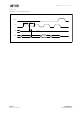
AS7262 − Detailed Description Detailed Description Figure 14: AS7262 Functional Block Diagram VDD1 VDD2 INT RX / SCL_S TX / SDA_S LED_IND 2 UART / I C LED_DRV I2C_ENB °C Spectral_ID Engine SPI Master MISO MOSI SCK CSN_SD Multi Spectral Sensor V B G Y O R RESN RC Osc 16MHz GND 6-Channel Visible Spectral_ID Detector The AS7262 6-channel Spectral_ID is a next-generation digital spectral sensor device.
AS7262 − Detailed Description Data Conversion Description AS7262 spectral conversion is implemented via two photodiode banks per device. Bank 1 consists of data from the V, G, B, Y photodiodes. Bank 2 consists of data from the G, Y, O, R photodiodes. Spectral conversion requires the integration time (IT in ms) set to complete. If both photodiode banks are required to complete the conversion, the 2 nd bank requires an additional IT ms. Minimum IT for a single bank conversion is 2.8 ms.
AS7262 − Detailed Description Figure 15: Photo Diode Array Photo Diode Array G Y B O V R Figure 16: Bank Mode and Data Conversion BANK Mode 0 One Conversion V, B, G, Y Integration Time BANK Mode 1 One Conversion G, Y, O, R Integration Time BANK Mode 2 1st Conversion Integration Time V, B, G, Y 2nd Conversion G, Y, O, R Integration Time ams Datasheet [v1-01] 2017-Mar-17 Page 15 Document Feedback
AS7262 − Detailed Description RC Oscillator The timing generation circuit consists of an on-chip 16MHz, temperature compensated oscillator, which provides the master clock for the AS7262. Temperature Sensor The temperature sensor is constantly measuring the on-chip temperature and enables temperature compensation procedures. Reset Pulling down the RESN pin for longer than 100ms resets the AS7262.
AS7262 − Detailed Description Electronic Shutter with LED_DRV Driver Control There are two LED driver outputs that can be used to control up to 2 LEDs. This will allow different wavelength light sources to be used in the same system. The LED output sink currents are programmable and can drive external LED sources: LED_IND from 1mA, 2mA, 4mA and 8mA and LED_DRV from 12.5mA, 25mA, 50mA and 100mA.
AS7262 − Detailed Description I²C Feature List • Fast mode (400kHz) and standard mode (100kHz) support. • 7+1-bit addressing mode. • Write format: Byte. • Read format: Byte. • SDA input delay and SCL spike filtering by integrated RC-components.
AS7262 − Detailed Description I²C Virtual Register Byte Write Pseudocode Poll I²C slave STATUS register; If TX_VALID bit is 0, a write can be performed on the interface; Send a virtual register address and set the MSB of the register address to 1 to indicate the pending write; Poll I²C slave STATUS register; If TX_VALID bit is 0, the virtual register address for the write has been received and the data may now be written; Write the data.
AS7262 − Detailed Description I²C Virtual Register Read Access I²C Virtual Register Byte Read shows the pseudocode necessary to read virtual registers on the AS7262. Note that in this case, reading a virtual register, the register address is not modified.
AS7262 − Detailed Description 4-Byte Floating-Point (FP) Registers Several 4-byte registers (hex) are used by the AS7262.
AS7262 − Detailed Description I²C Virtual Register Set Figure 20 provides a summary of the AS7262 I²C register set. Figures after that provide additional register details. All register data is hex, and all multi-byte entities are Big Endian (most significant byte is situated at the lowest register address). Multiple byte registers (2 byte integer, or, 4 byte floating point) must be read in the order of ascending register addresses (low to high).
AS7262 − Detailed Description Addr Name Sensor Calibrated Data Registers 0x14:0x17 V_Cal Channel V Calibrated Data (floating point) 0x18:0x1B B_Cal Channel B Calibrated Data (floating point) 0x1C:0x1F G_Cal Channel G Calibrated Data (floating point) 0x20:0x23 Y_Cal Channel Y Calibrated Data (floating point) 0x24:0x27 O_Cal Channel O Calibrated Data (floating point) 0x28:0x2B R_Cal Channel R Calibrated Data (floating point) ams Datasheet [v
AS7262 − Detailed Description Detailed Register Description Figure 21: HW Version Registers Addr: 0x00 HW_Version Bit Bit Name Default Access 7:0 Device Type 01000000 R Addr: 0x01 Bit Description Device type number HW_Version Bit Bit Name Default Access 7:0 HW Version 00111110 R Bit Description Hardware version Figure 22: FW Version Registers Addr: 0x02 FW_Version Bit Bit Name Default Access 7:6 Minor Version R Minor version [1:0] 5:0 Sub Version R Sub version Addr: 0x
AS7262 − Detailed Description Figure 23: Control Setup Register Addr: 0x04/0x84 Control_Setup Bit Bit Name Default Access Bit Description 7 RST 0 R/W Soft Reset, Set to 1 for soft reset, goes to 0 automatically after the reset 6 INT 0 R/W Enable interrupt pin output (INT), 1: Enable, 0: Disable 5:4 GAIN 0 R/W Sensor Channel Gain Setting (all channels) ‘b00=1x; ‘b01=3.
AS7262 − Detailed Description Figure 26: LED Control Register Addr: 0x07/0x87 LED Control Bit Bit Name Default Access 7:6 RSVD 0 R 5:4 ICL_DRV 00 R/W LED_DRV current limit ‘b00=12.
AS7262 − Detailed Description Figure 27: Sensor Raw Data Registers Addr: 0x08 Bit Bit Name 7:0 V_High V_High Default Access R Addr: 0x09 Bit Bit Name 7:0 V_Low Bit Name 7:0 B_High Default Access R Bit Name 7:0 B_Low Default Bit Name 7:0 G_High R Bit Name 7:0 G_Low Default Bit Name 7:0 Y_High R Bit Name 7:0 Y_Low ams Datasheet [v1-01] 2017-Mar-17 Bit Description Channel B Low Data Byte G_High Default Access R Bit Description Channel G High Data Byte G_Low Default Acc
AS7262 − Detailed Description Addr: 0x10 Bit Bit Name 7:0 O_High O_High Default Access R Addr: 0x11 Bit Bit Name 7:0 O_Low Bit Name 7:0 R_High Default Access R Bit Name 7:0 R_Low Page 28 Document Feedback Bit Description Channel O Low Data Byte R_High Default Access R Addr: 0x13 Bit Channel O High Data Byte O_Low Addr: 0x12 Bit Bit Description Bit Description Channel R High Data Byte R_Low Default Access R Bit Description Channel R Low Data Byte ams Datasheet [v1-01] 2017-Mar
AS7262 − Detailed Description Figure 28: Sensor Calibrated Data Registers Addr: 0x14:0x17 Bit Bit Name 31:0 V_Cal V_Cal Default Access R Addr: 0x18:0x1B Bit Bit Name 31:0 B_Cal Bit Name 31:0 G_Cal Default Access R Bit Name 31:0 Y_Cal Default Access R Bit Name 31:0 O_Cal Default Access R Bit Name 31:0 R_Cal ams Datasheet [v1-01] 2017-Mar-17 Bit Description Channel G Calibrated Data (floating point) Bit Description Channel Y Calibrated Data (floating point) O_Cal Default Acce
AS7262 − Detailed Description UART Interface If selected by the I²C_ENB pin setting, the UART module implements the TX and RX signals as defined in the RS-232 / V.24 standard communication protocol. It has on both, receive and transmit path, a 16 entry deep FIFO. It can generate interrupts as required. UART Feature List 1 • Full Duplex Operation (Independent Serial Receive and Transmit Registers) with FIFO buffer of 8 byte for each. • At a clock rate of 16MHz it supports communication at 115200 Baud.
AS7262 − Detailed Description AT Command Interface The microprocessor interface to control the Visible Spectral_ID sensor is via the UART, using the AT Commands across the UART interface. The 6-channel Spectral _ID sensor provides a text-based serial command interface borrowed from the “AT Command” model used in early Hayes modems.
AS7262 − Detailed Description Figure 31: AT Commands Command Response Description/Parameters Spectral Data per Channel ATDATA , , , , , OK ATCDATA , , , , , OK Read V, B, G, Y, O & R data. Returns comma-separated 16-bit integers. Read calibrated V, B, G, Y, O & R data. Returns comma-separated 32-bit floating point values.
AS7262 − Detailed Description Command Response Description/Parameters LED Driver Controls ATLED0= OK ATLED0 <100|0>OK ATLED1= OK ATLED1 <100|0>OK Sets LED_IND: 100=ON, 0=OFF Reads LED_IND setting: 100=ON, 0=OFF Sets LED_DRV: 100=ON, 0=OFF Reads LED_DRV setting: 100=ON, 0=OFF ATLEDC= OK Sets LED_IND and LED_DRV current LED_IND: bits 3:0; LED_DRV: 7:4 bits LED_IND: ‘b00=1mA; ‘b01=2mA; ‘b10=4mA; ‘b11=8mA LED_DRV: ‘b00=12.
AS7262 − Application Information Application Information Schematic Figure 32: AS7262 Typical Application Circuit 3V3 3V3 CSN_SD 7 14 VDD2 CSN_EE 6 1 /CS 2 RESN MISO 5 2 DO 16 GND MOSI 4 5 SCK 3 6 DI Flash CLKMemory 8 3 /WP 7 /HOLD 3V3 Vled 15 LED_DRV 18 LED_IND AS7262 I2C_ENB TX INT 11 RX/SCL_S 12 TX/SDA_S 13 INT NC NC NC NC NC 19 20 1 10 9 VCC 8 DNP RX 1uF GND 10K RST VDD1 4 100 nF 10uF 17 0R PCB Layout Figure 33: Typical Layout Routing In order to p
AS7262 − Package Drawings & Markings Package Drawings & Markings Figure 34: Package Drawings LGA AS7262 RoHS Green Note(s): 1.
AS7262 − PCB Pad Layout PCB Pad Layout Suggested PCB pad layout guidelines for the LGA device are shown. Figure 35: Recommended PCB Pad Layout Unit: mm 0.30 1.10 0.65 4.60 1 4.40 Note(s): 1. Unless otherwise specified, all dimensions are in millimeters. 2. Dimensional tolerances are ±0.05mm unless otherwise noted. 3. This drawing is subject to change without notice.
AS7262 − Mechanical Data Mechanical Data Figure 36: Tape & Reel Information Note(s): 1. Each reel contains 2000 parts.
AS7262 − Soldering & Storage Information Soldering & Storage Information Soldering Information The module has been tested and has demonstrated an ability to be reflow soldered to a PCB substrate. The solder reflow profile describes the expected maximum heat exposure of components during the solder reflow process of product on a PCB. Temperature is measured on top of component. The components should be limited to a maximum of three passes through this solder reflow profile.
AS7262 − Soldering & Storage Information Manufacturing Process Considerations The AS7262 package is compatible with standard reflow no-clean and cleaning processes including aqueous, solvent or ultrasonic techniques. However, as an open-aperture device, precautions must be taken to avoid particulate or solvent contamination as a result of any manufacturing processes, including pick and place, reflow, cleaning, integration assembly and/or testing. Temporary covering of the aperture is allowed.
AS7262 − Soldering & Storage Information Floor Life The module has been assigned a moisture sensitivity level of MSL 3.
AS7262 − Ordering & Contact Information Ordering & Contact Information Figure 39: Ordering Information (1) Ordering Code Package Marking Description Delivery Form Delivery Quantity AS7262-BLGT 20-pin LGA AS7262 6-Channel Visible Spectral_ID Device with Electronic Shutter and Smart Interface Tape & Reel 2000 pcs/reel Note(s): 1. Required companion serial flash memory (must be ams verified) is ordered from the flash memory supplier (e.g. AT25SF041-SSHD-B from Adesto Technologies). 2.
AS7262 − RoHS Compliant & ams Green Statement RoHS Compliant & ams Green Statement RoHS: The term RoHS compliant means that ams AG products fully comply with current RoHS directives. Our semiconductor products do not contain any chemicals for all 6 substance categories, including the requirement that lead not exceed 0.1% by weight in homogeneous materials. Where designed to be soldered at high temperatures, RoHS compliant products are suitable for use in specified lead-free processes.
AS7262 − Copyrights & Disclaimer Copyrights & Disclaimer Copyright ams AG, Tobelbader Strasse 30, 8141 Premstaetten, Austria-Europe. Trademarks Registered. All rights reserved. The material herein may not be reproduced, adapted, merged, translated, stored, or used without the prior written consent of the copyright owner. Devices sold by ams AG are covered by the warranty and patent indemnification provisions appearing in its General Terms of Trade.
AS7262 − Document Status Document Status Document Status Product Preview Preliminary Datasheet Datasheet Datasheet (discontinued) Page 44 Document Feedback Product Status Definition Pre-Development Information in this datasheet is based on product ideas in the planning phase of development.
AS7262 − Revision Information Revision Information Changes from 1-00 (2016-Dec-16) to current revision 1-01 (2017-Mar-17) Updated Figure 12 and notes below Page 11 Note(s): 1. Page and figure numbers for the previous version may differ from page and figure numbers in the current revision. 2. Correction of typographical errors is not explicitly mentioned.
AS7262 − Content Guide Content Guide Page 46 Document Feedback 1 1 2 2 General Description Key Benefits & Features Applications Block Diagram 3 5 6 8 11 12 Pin Assignments Absolute Maximum Ratings Electrical Characteristics Timing Characteristics Optical Characteristics Typical Optical Characteristics 13 13 14 16 16 16 16 17 17 17 18 18 19 20 20 21 22 24 30 30 30 30 30 31 Detailed Description 6-Channel Visible Spectral_ID Detector Data Conversion Description RC Oscillator Temperature Sensor Reset In
AS7262 − Content Guide 41 42 43 44 45 ams Datasheet [v1-01] 2017-Mar-17 Ordering & Contact Information RoHS Compliant & ams Green Statement Copyrights & Disclaimer Document Status Revision Information Page 47 Document Feedback
Mouser Electronics Authorized Distributor Click to View Pricing, Inventory, Delivery & Lifecycle Information: ams: AS7262