
Datasheet
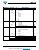

VEML7700
www.vishay.com
Vishay Semiconductors
Rev. 1.0, 19-Nov-15
2
Document Number: 84286
For technical questions, contact: sensorstechsupport@vishay.com
THIS DOCUMENT IS SUBJECT TO CHANGE WITHOUT NOTICE. THE PRODUCTS DESCRIBED HEREIN AND THIS DOCUMENT
ARE SUBJECT TO SPECIFIC DISCLAIMERS, SET FORTH AT www.vishay.com/doc?91000
Note
• rem_1: light source: white LED
rem_2: light conditions: dark
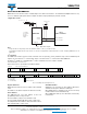
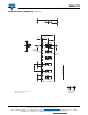
CIRCUIT BLOCK DIAGRAM
Fig. 1 - Block Diagram
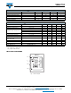
ABSOLUTE MAXIMUM RATINGS (T
amb
= 25 °C, unless otherwise specified)
PARAMETER TEST CONDITION SYMBOL MIN. MAX. UNIT
Supply voltage V
DD
04V
Operation temperature range T
amb
-25 +85 °C
Storage temperature range T
stg
-25 +85 °C
Total power dissipation T
amb
≤ 25 °C P
tot
-50mW
Junction temperature T
j
- 100 °C
BASIC CHARACTERISTICS (T
amb
= 25 °C, unless otherwise specified)
PARAMETER TEST CONDITION SYMBOL MIN. TYP. MAX. UNIT
Supply voltage V
DD
2.5 3.3 3.6 V
Shut down current (rem_2) V
DD
is 3.3 V I
sd
-0.5-μA
Operation mode current (rem_2)
V
DD
is 3.3 V, PSM = 11, refresh time 4100 ms I
DD
-2-μA
V
DD
is 3.3 V, PSM = 00, refresh time 600 ms I
DD
-8-μA
V
DD
is 3.3 V, PSM_EN = 0, refresh time 100 ms I
DD
45 - μA
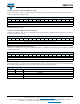
I
2
C clock rate range f
SCL
10 - 400 kHz
I
2
C bus input H-level range V
DD
is 3.3 V V
ih
1.3 - 3.6 V
I
2
C bus input L-level range V
DD
is 3.3 V V
il
--0.4V
Digital current out
(low, current sink)
I
ol
3-?mA
Digital resolution (LSB count) with ALS_SM = “01” - 0.005 - lx/step
Detectable minimum illuminance with ALS_SM = “01” E
V min.
-0.01- lx
Detectable maximum illuminance with ALS_SM = “10” E
V max.
- 167 000 - lx
Dark offset (rem_2) with ALS_SM = “01” - 3 - step
1
2
3
V
DD
SCL
4
GND
VEML7700
Oscillator
ALS-PD
Output buffer
I
2
C interface
Timing
controller
Temperature
sensor
Low pass
lter
SDA