Wireless Module SparkLAN WPEB-265AXI(BT) [B33] & AP12275_PB33 WPEB-265AXI(BT) [B18] & AP12275_PB18 WPEB-265AXI(BT) [R33] & AP12275_PR33 WPEB-265AXI(BT) [R18] & AP12275_PR18 HW User manual Version 0.0 Revision History Date 2020/12/30 Revision Content Initial released Revised By Version Wayne 0.
Wireless Module Contents Revision History ............................................................................................................... 0 1. WPEB-265AXI(BT) [XXX] Series Hardware User Manual Introduction ................... 2 1.1. Module Block Diagram ..................................................................................... 2 1.2. External Reference Circuit ............................................................................... 3 2. PCB Layout Guide ....................
Wireless Module 1. WPEB-265AXI(BT) [XXX] Series Hardware User Manual Introduction This document provides customers with considerations for the hardware design of WPEB-265AXI(BT) [XXX] series. It includes hardware block diagram, reference design, PCB layout, and PCB stack up, which will be explained in detail below. 1.1. Module Block Diagram SparkLAN WPEB-265AXI(BT) [ B 33 ] & Ampak AP12275_ P B 33 GPIOs Voltage Level 18: Typ. 1.8V (1.62V~1.98V) 33: Typ. 3.3V (3.0V~3.
Wireless Module 1.2. External Reference Circuit Connected to HOST I/O VIO Voltage Level [B33], [R33] : Typ.3.3V (3.0V~3.6V) [B18], [R18] : Typ.1.8V (1.62V~1.98V) Turn on the Wi-Fi function at default. WL_REG_ON WLAN HOST_PCIE_RDP C121 0.1uF PCIE_TDP HOST_PCIE_RDN C122 0.
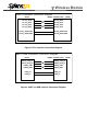
Wireless Module PCIe interface conection diagram WPEB-265AXI(BT) [XXX] HOST PCIe_TDP PCIe_TDN PCIe_RDP PCIe_RDN PCIE_REFCLKP PCIE_REFCLKN PCIE_RDN PCIE_RDP PCIE_TDN PCIE_TDP PCIE_REFCLKP PCIE_REFCLKN Figure3. PCI-e Interface Connection Diagram UART & PCM interface conection diagram HOST UART_CTS_N UART_RTS_N UART_TXD UART_RXD USB_D+ USB_D- WPEB-265AXI(BT) [XXX] UART_CTS_N UART_RTS_N UART_TXD UART_RXD USB_D+ USB_D- Figure4.
Wireless Module 2. PCB Layout Guide 2.1. PCI-e Layout Guide 1. The PCI-e differential pair signals impedance target is 100±20% ohms 2. 3. 4. 5. 6. 7. impedance. Do not place probe or test points on any high-speed differential signal. Do not route high-speed traces under or near crystals, oscillators, clock signal generators, switching power regulators, mounting holes, magnetic devices, or ICs that use or duplicate clock signals. The traces routing don't be 90° angle.
Federal Communication Commission Interference Statement: This equipment has been tested and found to comply with the limits for a Class B digital device, pursuant to part 15 of the FCC Rules. These limits are designed to provide reasonable protection against harmful interference in a residential installation. This equipment generates, uses and can radiate radio frequency energy and, if not installed and used in accordance with the instructions, may cause harmful interference to radio communications.
the maximum permissible gain indicated. Antenna types not included in this list that have a gain greater than the maximum gain indicated for any type listed are strictly prohibited for use with this device. Unique antenna connector (RP-SMA) must be used on the Part 15 authorized transmitters used in the host product. Antenna Type Antenna Model Maximum Gain (dBi) 2.4 GHz 5GHz Dipole AD-103AG 2.02 dBi 2.03 dBi Dipole AD-302N 3.14 dBi 2.73 dBi Dipole AD-303N 3.14 dBi 3.
Industry Canada statement: This device complies with Industry Canada license-exempt RSSs. Operation is subject to the following two conditions: 1) This device may not cause interference, and 2) This device must accept any interference, including interference that may cause undesired operation of the device. Le présent appareil est conforme aux CNR d’Industrie Canada applicables aux appareils radio exempts de licence.
pour l’exploitation point à point et non point à point, selon le cas. Radiation Exposure Statement: This equipment complies with IC radiation exposure limits set forth for an uncontrolled environment. This equipment should be installed and operated with minimum distance 20cm between the radiator & your body. Déclaration d’exposition aux radiations: Cet équipement est conforme aux limites d’exposition aux rayonnements IC établies pour un environnement non contrôlé.
Cette étiquette extérieure peut utiliser un libellé comme celui-ci: “ Contient IC: 6158A-PEB265AXIBT“. Plaque signalétique du produit final: Le produit final doit être étiqueté dans un endroit visible avec l'inscription suivante: "Contient des IC: 6158A-PEB265AXIBT ". Manual Information To the End User: The OEM integrator has to be aware not to provide information to the end user regarding how to install or remove this RF module in the user’s manual of the end product which integrates this module.
different operational conditions for a stand-alone modular transmitter in a host, host manufacturer have to consult with module manufacturer for the installation method in end system. l'hôte doit utiliser l'instrument uniquement dans des dispositifs qui répondent à la fcc / (catégorie d'exposition rf mobile, ce qui signifie le dispositif est installé et utilisé à une distance d'au moins 20 cm de personnes.