SERVICE MANUAL MODEL : VM-1201 REVISION : A0 DATE : MAY. 21.
WARNING ========== For continuous protection against radiation, shock and flame, replace only with same type and rating components specified in the approved sheets. Disclaimer Speco Technologies makes no representation or warranties, either expressed or implied, with respect to the contents hereof and specifically disclaims any warranties, merchantability or fitness for any particular purpose.
2.4 VERTICAL DEFLECTION BLOCK.........................................……………………..………... 8 2.5 HORIZONTAL DEFLECTION BLOCK.............................……………………............……... 8 3. TROUBLESHOOTING INSTRUCTIONS............................................……………...…….….. 9 3.1 NO DISPLAY, NO POWER.......................…………………………………………………….. 9 3.2 NO DISPLAY, (POWER OK)............………………………………………………………….. 9 3.3 NO DISPLAY, (NO ASTER) ……………………………………………..........…………….. 10 3.
Audience This service manual is primarily for system / service engineers, distributors and dealers. It carries the assumption that the reader understands the basic operating concepts. Purpose This manual contains reference data for Speco Technologies monitor. It gives information regarding the operating principles of monitors, as well as technical service and maintenance information. 1.
1.1.2 Signal Input Requirements ‧ Connector For CVBS:BNC terminal Type:composite video input Level:1.0Vp-p Synchronous:0.3 V Luminance:0.7V Polarity:Positive bright Impedance:75 ohms 1.1.3 Power Input Requirements ‧ Operating Voltage Range:90 ~ 264 VAC at 50 / 60 ±3Hz ‧ Input Current at 90 VAC Operating:0.5 Amps rms. maximum ‧ Input Current at 264 V Operating:0.3 Amps rms. maximum ‧ Power consumption Normal operation:30 Watts maximum 1.
• Temperature :25 ±5℃ • Magnetic field :No additional magnetic field in near side • AC line Input :100 ~ 240 VAC ±10%, 50/60 ±3Hz • Warm-up Time :30 minutes min. after power on and signal applied • Ambient light :400 to 600 lux. 1.2.
‧ Picture geometry:≦ 2.5% ‧ Picture centering:≦ 6mm ‧ Size stability:Picture luminance from 5 FL to max., the size shall be less than 2.5% (with full white pattern) ‧ Swing and jitters:Swing and jitters are not allowed (viewed at 50cm from eyes to screen). ‧ Focus:(viewed at 50cm from eye to screen, contrast adjusted to set luminance at 20 FL with full white pattern, brightness set at raster just disappeared) Inspect full character pattern, all characters should be distinguished. 1.
This section describes each functional block of the monitor. 2.1 Main Power Supply Block • AC power input:AC socket • Line input noise / EMI filtering:Line filter T902 ; X-Cap C901, C902. Y-Cap C903, C904, C905. • Over current protection:Fuse • Power on/off control:Power switch • AC to DC conversion and filtering:Diode D901, Capacitor C906 • Start-up circuit:R914, C914.
• Snubber circuit:Snubber C907, D902, R902. • Primary side self-powering circuit:D903,C914. • Output 13.5 volts for vertical & horizontal drive circuits:D904, C915. • Output 27.5volts for horizontal deflection circuit:D906 ,C916. 2.2 Video input block • Signal input buffering and switch ‧ CVBS Input buffer :Q201 & R201,R202. • Video filter & output stage. ‧ Video input:Through C202 to W202 (Contrast VR ) and differential amplifier Q202, Q203.
black level is stored at pin7 by C404. The slicing level is stored at pin6 by C403 and decided by R403. 2.3.4 Phase detector: The phase detector circuit is connected to pin8. The circuits are activated depending on the voltage of pin18 and the state of the Sync pulse noise detection circuit, C405, C406, R405. 2.3.5 Supply (pin9, 10 and 16): U401 can start operating by application of a very low supply current into pin16.
• Flyback generator: ‧ U301 pin6 is the output of the flyback generator that when driven, jumps from low to high condition C305 transfers the jump to pin3 • Vertical size control:VR301, R312, R308. 2.5 Horizontal Deflection Block • Horizontal drive buffering:Driving source-U401 pin11. Driving transistor-Q40, to pull high the driving waveform to drive the Q401(MOS FET).
3.1.5 If driving pulses at U901 pin6 and drain of Q901 are correct but voltage at U901 pin 7 low than threshold voltage --causing U901 to stop and restart periodically, check and repair following circuits. Power transformer T901 bad; D903 short-circuit/opened. 3.2 No Display, power output normal. 3.2.1 Check and fix FBT B+:If no B+(27.5V)on pin2 of FBT replace D906, C916. 3.2.2 Check driving output voltage:0 or very low check and replace Q402, Q401. 3.2.3 Power off monitor. Check yoke connection.
Appendix A. Spare Parts List Location F901 D901 D902 D501, D502 D903, D904, D301 D906, D401 Q901 Q201, Q202, Q206, Q402, Q501 Q205 Q502 Q203, Q204 U401 Parts Number 28-1100-0006 06-3100-0005 06-1100-0001 06-1100-0023 06-1100-0014 06-1100-0058 08-3100-0011 08-1100-0003 08-1100-0001 08-1100-0002 08-1100-0081 09-4100-0007 Description Fuse, 2A/250V, slow blow Diode 3A, 600V, RS407 Diode, 1.
Appendix B. Schematics and PCB Layout Diagram 1. Schematics Page 1 -- Main Board, Video Board. 2. Schematics Page 2 – Power Supply, Video Amplifier 3. PCB Layout -- Video Board, Circuit Trace 4.
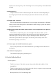
A B C 1 PLUG AC SOCKET W902 R911 3.9K SYNC- SYNC+ VR901 SVR 1KB C912 104/50V 2 R901 560K C902 0.1U/250V C904 472/400V Vfb IC3842 R907 390 R909 27K R908 47 D903 FR105 C914 EC 100U/25V C906 47U/400V D901 3A/600V 2 R906 1K C909 1000P D905 1N4148 R905 18 3 C910 562/100V Ise OUT 6 C903 472/400V COMP U901 C914 EC 100U/25V EE-25 T902 R903 PEI 103 1M 1 R910 27K C911 C901 .1U/250V 2.5A/250V F901 2 R904 .
A B C 1 R312 33 C304 .047 R308 100 VR301 300B V-SIZE R306 1.5 1W R311 330K VR401 H-HOLD R304 1K R302 2.2K C303 .047 C309 4.7U R315 470 2700P 1 1 7 R303 5.6K D301 1N4002 C302 472 C411 103 18 R217 15K R301 4.7K 2 U301 IC TDA8712 2 C409 17 2 R411 30K 16 3 U401 C304 2200P TDA2579 C306 104 C308 1000U/25V 180 1/2W R307 R408 12K R406 18K 12.9V C311 .022 C402 150P R305 1 5 2.7 2W R313 C305 100U/35V C301 .15 R411 33K C408 1U R409 270 3 R410 2.2K 12.