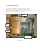
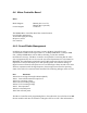
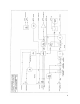
4. Technical Description The internal design of the MX800 is of a modular nature allowing for simple configuration and maintenance while ensuring minimal downtime. For reference purposes, the top view of a typical MX800 with top cover removed is shown below. The standard unit without speaker and microphone is illustrated. PA Module Exciter Module Receiver Module Micro Controller Board MX800 top view.
4.1. Exciter Module Refer. Exciter Block Diagram: Exciter Circuit Diagram: TX VCO Circuit Diagram: BD002 CS002-1 CS004-1 (Bands A to Q) RF from the VCO on SKU-1 at a nominal level of+3dBm is applied to the fractional-N synthesizer ICI0 main divider input. This signal is compared with the reference oscillator frequency and the correction voltage from the synthesizers charge pump output is filtered then amplified by the non inverting low noise op amp IC9A.
resulting in a flat VF response. 4.2. Receiver Module Refer: Receiver Block Diagram: Receiver Front End Circuit Diagram: Receiver IF Circuit Diagram: RX VCO Circuit Diagram: BD001 CS003-2 CS003-1 CS005-1 (Band A to Q) CS012-1 (Band R to X) The receive signal from the antenna enters on CN1 a 3 section Bandpass filter which provides the initial filtering for the front end amplifier.
so as to provide a wide tuning range voltage to the frequency control varicaps located on the VCO board. Frequency programming data for the receiver is sent to the synthesizer chip from the Micro Controller via the a serial data line on SKD-18 under the control of the Clock (SKD- 15) and Strobe (SKD- 17) lines The local oscillator signal to the mixer is controlled by the Micro Controller through an enable signal on SKD-8.
4.4. Micro Controller Board Refer: Block Diagram Circuit Diagram BD003 ( Rev A to I-D BD005 (Rev I upwards) CS001-1/6 The MX800 Micro Controller Board has 4 main functions Overall radio management TX and RX signal processing RF power control User interface 4.4.1.
communicated to the Receiver and Exciter modules by way of bussed data and clock lines on SKC/D-18 and SKC/D-15 (Exciter/Receiver) and an individual module strobe on SKC/D-17. A lock detect signal from each module on SKC/D-16 is read by the micro controller. In addition to the synthesizer programming bus an I2C bus goes to each of the modules. This bus is currently unused. IC25 is a non predictive, full duplex CTCSS encoder/decoder which is under the control of the microprocessor. 4.4.2.
set up using the Configure screen of MXTOOLS. The output of this final stage is fed to two microprocessor controlled digipots which serve to adjust the modulating signal level to the VCO and the reference oscillator. A third digipot is used to provide an offset null for the reference oscillator center frequency. Adjustment of these levels is also by way of MXTOOLS using the Channel Edit screen. 4.4.3. RX Signal Processing.
connected to the wiper of the digipot, is set up with a reference voltage. The detected actual PA forward power is fed to the inverting input oflC23A. The error voltage at the output of IC23A is fed to the exciter output power control circuit via SKC-4 and the action of the control loop is to set the RF power such that the actual detected volts equals the reference volts. The digipot setting is static for each channel unless the required forward power is changed.