
Technical Description
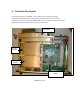
4.1. Exciter Module
Refer.
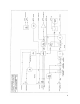
Exciter Block Diagram: BD002
Exciter Circuit Diagram: CS002-1
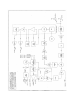
TX VCO Circuit Diagram: CS004-1 (Bands A to Q)
RF from the VCO on SKU-1 at a nominal level of+3dBm is applied to the fractional-N
synthesizer ICI0 main divider input. This signal is compared with the reference oscillator
frequency and the correction voltage from the synthesizers charge pump output is filtered
then amplified by the non inverting low noise op amp IC9A. This correction voltage is
fed back to the VCO to maintain loop lock as well as being fed to the Micro Controller
via SKD-14. A lock detect signal from IC10 is also fed to the Micro Controller via SKD-
16.
The op amp uses a 25 volt power supply (generated on the Micro Controller) so as to
provide a wide tuning range voltage to the frequency control varicaps located on the
VCO
board. Frequency programming data for the exciter is sent to the synthesizer chip from
the Micro Controller via a serial data line on SKD-18 under the control of the Clock
(SKD-15) and Strobe (SKD-17) lines.
Provision is made for the optional injection of an external reference frequency. If this
option is selected CN3 is fitted and X1 is not fitted. Components R30 and TR7 are also
omitted.
A second RF output from the VCO on SKT-6 also at +3dBm is used as the main transmit
RF amplifier signal source. This main signal is first buffered by a very high isolation
circuit consisting ofa 10dB pad and a MMIC amplifier (IC1). The signal is further
amplified by IC2 and a variable gain wide band amplifier with 40dB control range and
power output of 300mW. The drive power of this stage is used to set the output power to
the main power amplifier under the control of the DC voltage on SKD-4 from the Micro
Controller board.
The VCO boards and synthesizer circuits are the same for the exciter and receiver
modules. The VCO consists ofa 10mm ceramic coaxial resonator with common base
oscillator for low phase noise for bands 805-960 MHz. Frequencies below 520 MHz use
an LC tank circuit. The power supply to the VCO consists of an 8 volt regulator and
active filter for maximum noise rejection. It is controlled by the Micro Controller through
SKD-7 which connects to switch TR6. For standard modulation, transmit audio is fed on
SKD-8 to the conventional point of the VCO varactor. For 2 point modulation, audio is
also fed via SKD-19 to the voltage control pin of the VC-TXCO, this in effect cancels out
the PLL error that would otherwise have occurred for low audio frequencies, hence