
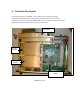
Technical Description
resulting in a flat VF response.
4.2. Receiver Module
Refer:
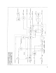
Receiver Block Diagram: BD001
Receiver Front End Circuit Diagram: CS003-2
Receiver IF Circuit Diagram: CS003-1
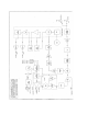
RX VCO Circuit Diagram: CS005-1 (Band A to Q)
CS012-1 (Band R to X)
The receive signal from the antenna enters on CN1 a 3 section Bandpass filter which
provides the initial filtering for the front end amplifier. The front end amplifier IC12 is a
broad band high performance MMIC with a gain of 18dB, noise figure of 4dB and 3rd
order intermodulation intercept of+36dB. This is followed by a 4dB pad and a second 3
section BPF, and a high level double balanced mixer M1.
The receiver uses high side local oscillator injection for bands A to I and low side
injection for all other bands. RF from the VCO main output on SKT-6 is buffered and
amplified to + 17dBm by IC4 and injected in the high level mixer which down converts
the signal to the first IF frequency of 90 MHz (45MHz for bands A to D3). This IF signal
from the mixer is terminated by a bi-directional constant impedance network and is then
amplified by a hipolar amplifier TR2 with a gain of 15dB and 3rd order intermodulation
intercept +35dB. This provides a high degree of intermodulation rejection for the
receiver. This stage is followed by a 4 pole 90 MHz crystal filter FL3A/B with its
associated matching networks. The signal is further amplified and filtered by a transistor
amplifier TR3 and its associated 2 pole crystal filter FL4 before being fed into the main
IF demodulator chip IC 1 with a second IF frequency of 455kHz. The resulting audio is
passed out to the Micro Controller board on SKD-3. The Received Signal Strength
Indication (RSSI) from IC1 is buffered by IC5A and connected to the Micro Controller
board via SKD-4.
RF from the VCO on SKU-1 at a nominal level of+3dBm, is applied to the fractional-N
synthesizer (IC10) main divider input. This signal is compared with the reference
oscillator frequency and the correction voltage from the synthesizer's charge pump output
is filtered then amplified by the non inverting low noise op amp (ICI 1A). This correction
voltage is fed back to the VCO to maintain loop lock as well as being fed to the Micro
Controller via SKD44. A lock detect signal from IC10 is also fed to the Micro Controller
via SKD-I6. The op amp uses a 25 volt power supply (generated on the Micro Controller)