NRM7292D User Manual Ultra-low power & Long-range Wi-Fi Module Ver 1 JUL 27, 2022 SRF Co.,Ltd ___________________________________________________________________________________ © Copyright SRF 20202. All rights reserved.
Notice SRF continually work to improve the performance and quality of products. The information in this document has been carefully checked and is believed to be entirely accurate at the release time. Please, ensure that SRF’s product must be working within this specification. But, SRF assumes no responsibility, however, for possible errors or missing, or for any result from the use of the information contained documents.
Contents 1 Overview ...................................................................................................................................... 2 1.1 Applications .................................................................................................................................. 2 1.2 NRM7292D module features ........................................................................................................3 3 Pin Description ....................................................
List of Tables Table 3.1 Table 5.1 Table 5.2 Table 5.3 Table 6.1 Table 6.2 Table 6.3 Table 6.4 Table 6.5 NRM7292D signal description............................................................................................... 6 NRM7292D absolute maximum rating ................................................................................. 9 NRM7292D operating condition ........................................................................................... 9 NRM7292D current consumption ............
List of Figures Figure 1.1 NRM7292D pictures.............................................................................................................. 2 Figure 3.1 NRM7292D module pinout (top view).................................................................................. 5 Figure 4.1 Antenna Connection on EVK ................................................................................................. 8 Figure 7.1 Tape information .............................................................
NRM7292D NRM7292D Specification (US ) Page | 2 1 Overview IEEE 802.11ah is a new Wi-Fi standard operating in the Sub 1GHz license-exempt band, offering longer range and lower power connectivity necessary for internet of things (IoT) applications. NRM7292D contains external RF front end module (FEM) which can increase transmission power up to 23 dBm. Onboard serial flash can be used for OTA software development and with internal 32KB cache memory, it can support execution in place (XIP) feature.
NRM7292D NRM7292D Specification (US) Page | 3 1.2 NRM7292D module features The main features of NRM7292D are represented as follows: • Standard ▪ IEEE Std 802.
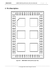
NRM7292D NRM7292B Specification (US) User Manual Page | 5 53 54 55 56 57 58 59 60 61 62 63 65 64 3 Pin Description 68 7 46 8 45 9 44 10 43 11 42 12 41 13 40 14 39 15 38 16 37 17 36 18 35 19 34 20 33 66 Figure 3.1 32 47 31 6 30 48 29 5 28 49 27 4 26 50 25 3 24 51 23 2 22 52 21 1 67 NRM7292D module pinout (top view) ___________________________________________________________________________________ © Copyright SRF 2020.
NRM7292D NRM7292D Specification (US) User Manual Page | 6 Table 3.
NRM7292D NRM7292D Specification (US) User Manual Page | 7 34 GP_11_UART1_TX I/O UART Channel1 Tx 35 GP_10_GPIO I/O 36 GP_09_GPIO I/O Multiple purpose (GPIO,I2C,PWM,SPI, Ext-INT) 37 GP_17_I2C_SDA I/O I2C_SDA 38 GP_16_I2C_SCL I/O I2C_SCL 39 GP_15_SSP0_CLK O SPI0_Clock 40 PD_14_SSP0_CS O SPI0_Chip Enable(active low) 41 PD_13_SSP0_MOSI O SPI0_Master out slave in 42 PD_12_SSP0_MISO I SPI0_Master in Slave out 43 RESET I Reset (active high) 44 GROUND 45 JTAG_TRSTN I
NRM7292D NRM7292D Specification (US) User Manual Page | 8 4 Antenna Connection 4.1 Antenna Connection An external Antenna is connected through the SMA type connector. It’s connected to Pad # 62 (RF_ANT) of NRM7292D through the PCB trace of 50ohm impedance. ⚫ Antenna Requirements - Connection Type: External Antenna (SMA connector) - Frequency Range : 902~928MHz - Input Impedance: 50ohm - Gain: Avg 0dBi (Max <1.68dBi) Please refer to NRM7292 EVK which use 900MHz Dipole Antenna as bellow.
NRM7292D NRM7292D Specification (US) User Manual Page | 9 5 Operating Condition 5.1 Absolute Maximum Rating Table 5.1 NRM7292D absolute maximum rating Symbol Min Max Unit Storage Temperature -40 +125 ℃ VDD_FEM -0.5 5.25 V VBAT -0.5 3.8 V VDDIO -0.5 3.8 V Supply Voltage ✓ NOTE : Stresses above those listed in Absolute Maximum Rating may cause permanent device failure. Functionality at or above these limits is not implied.
NRM7292D NRM7292D Specification (US) User Manual Page | 10 5.3 Current consumption Table 5.3 NRM7292D current consumption MODE Band (MHz) VDDIO (mA) VBAT (mA) VDD_FEM (mA) Tx @ 17 dBm (VDD_FEM = 3.3V) 0.5 33 148 Tx @ 17 dBm (VDD_FEM = 4.0V) 0.5 33 153 Tx @ 20 dBm (VDD_FEM = 3.3V) 0.5 33 177 0.5 33 184 Continuous Rx @ -80 dBm (VDD_FEM = 3.3V) 0.5 33 7 Continuous Rx @ -80 dBm (VDD_FEM = 4.0V) 0.5 33 7 0.6(uA) 27(uA) 0.4(uA) DUT Status 802.
NRM7292D NRM7292D Specification (US) User Manual Page | 11 6 11ah WLAN RF Specifications and Performance 6.1 Transmitter Specifications Table 6.
NRM7292D NRM7292D Specification (US) User Manual Page | 12 Baseband Filters for Receiver (Analog + Digital Filter) Baseband -3dB Low-pass Corner Frequency (Controllable) 1 MHz channel 2 MHz channel 4 MHz channel 0.5 1.0 2.0 MHz MHz MHz ✓ Note: Unless otherwise specified, TA.=27℃, VBAT=2.6 to 3.6V, VDD_FEM=4.0V. RF input/outputs specifications are referenced to device pins and do not include 1dB loss from EV kit OCB and SMA connector.
NRM7292D NRM7292D Specification (US) User Manual Page | 13 6.4 Receiver Performance 6.4.1 Receiver Sensitivity Table 6.4 Sensitivity (minimum input level) Band BW Rate Modulation/Coding Rate Conditions kbps 1 MHz 902~ 928MHz 2 MHz 4 MHz Chip Port Specification [dBm] Min 300 BPSK 1/2 600 QPSK 1/2 900 1200 1800 2400 2700 3000 150 QPSK 3/4 16QAM 1/2 16QAM 3/4 64QAM 2/3 64QAM 3/4 64QAM 5/6 BPSK 1/2 rep.
NRM7292D NRM7292D Specification (US) User Manual Page | 14 6.4.2 Adjacent Channel Rejection (ACR) Table 6.5 ACR Band BW Rate Modulation/Coding Rate kbps 1 MHz 902~ 928MHz 2 MHz 4 MHz ACR [dB] Conditions Min Typ 300 BPSK 1/2 36 600 900 1200 1800 2400 2700 3000 150 QPSK 1/2 QPSK 3/4 16QAM 1/2 16QAM 3/4 64QAM 2/3 64QAM 3/4 64QAM 5/6 BPSK 1/2 rep.
NRM7292D NRM7292D Specification (US) User Manual Page | 15 7 Packing Specification 7.1 Dimensions of Tape Figure 7.1 Tape information 7.2 Taping Diagrams Feeding Direction Pin1 Marking Feeding Hole Figure 7.2 Device orientation on tape ___________________________________________________________________________________ © Copyright SRF 2020. All rights reserved.
NRM7292D NRM7292D Specification (US) User Manual Page | 16 7.3 Box Information Figure 7.3 Box dimension 7.4 Label Information - Reel / AL Bag / Inner Box Device Part Number Vendor Module maker Lot Number Module Lot Quantity Moisture sensitivity level Halogen free mark RoHS compliant mark Figure 7.4 Label information ___________________________________________________________________________________ © Copyright SRF 2020. All rights reserved.
NRM7292D NRM7292D Specification (US) User Manual Page | 17 7.5 Packing Process Figure 7.5 Packing process ___________________________________________________________________________________ © Copyright SRF 2020. All rights reserved.
NRM7292D 8 NRM7292D Specification (US) User Manual Page | 18 SMT Temperature Sequence (Pb-free) Figure 8.1 Reflow profile ___________________________________________________________________________________ © Copyright SRF 2020. All rights reserved.
NRM7292D NRM7292D Specification (US) User Manual Page | 19 9 Revision History Revision No Ver 1.0 Date 7/27/2022 Comments Initial version for customer release created ___________________________________________________________________________________ © Copyright SRF 2020. All rights reserved.
FCC Compliance Statement This device complies with part 15 of the FCC rules. Operation is subject to the following two conditions: (1) This device may not cause harmful interference, and (2) this device must accept any interference received, including interference that may cause undesired operation. FCC Interference Statement This equipment has been tested and found to comply with the limits for a Class B digital device, pursuant to part 15 of the FCC Rules.
Information on test modes and additional testing requirements a) The modular transmitter has been fully tested by the module grantee on the required number of channels,modulation types and modes, it should not be necessary for the host installer to retest all the available transmitter modes or settings.
- Appropriate labels must be affixed to the product that complies with applicable regulations in all respects. The regulatory label on the final system must include the statement: “Contains FCC ID: 2A32R-NRM7292D”. 1. The module is limited to OEM installation ONLY. 2. OEM integrators are responsible for ensuring that the end-user has no manual instructions to remove or install module. 3. The module is limited to installation in mobile or fixed applications, according to Part 2.1091(b). 4.