
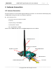
User's Manual


NRM7292D NRM7292D Specification (US) User Manual P a g e | 11
___________________________________________________________________________________
© Copyright SRF 2020. All rights reserved.
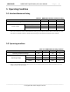
6 11ah WLAN RF Specifications and Performance
6.1 Transmitter Specifications
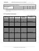
Table 6.1 Transmitter Spec/Feature (RF)
Parameter Conditions Min Typ Max Unit
RF Output Frequency Range
(1)
902 928 MHz
EVM Compliant Output Power 15 Mbps (MCS7, 4 MHz BW) 20 dBm
EVM at 0 dBm output power -35 dB
Transmitter Spurious Signal
Emissions
< 700 MHz <-36
dBm/
MHz
> 1 GHz <-45
RF Output Return Loss Single ended output port -10 dB
Output 1dB Gain Compression 0.4 MHz CW signal input 27 dBm
Gain Control Range 30 dB
Gain Control Step 1 dB
Unwanted Sideband
Over RF channel, RF frequency, and
baseband frequency at 0 dBm output
power
<-40 dBc
✓ Note: Unless otherwise specified, TA.=27℃, VBAT=2.6 to 3.6V, VDD_FEM=4.0V. RF input/outputs specifications are referenced
to device pins and do not include 1dB loss from EV kit OCB and SMA connector.
(1) RF output frequency range depends on RF SAW filter on the module. The NRC7292 chipset by itself can support frequency range
from 750 to 950 MHz.
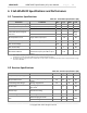
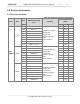
6.2 Receiver Specifications
Table 6.2 Receiver Spec/Feature (RF)
Parameter Conditions Min Typ Max Unit
RF Input Frequency Range
(1)
902 928 MHz
RF Input Return Loss
For LNA high/mid/low gain
modes
-10 -12 -15 dB
Total Voltage Gain Range Analog + Digital Gain -10 92 dB
RF Gain Step
From high gain mode to medium
gain mode
6 dB
RX Gain Step From RF to Analog 1 dB
DSB Noise Figure LNA max gain mode 3.5 dB
IIP3
LNA with high gain mode -17
dBm
LNA with low gain mode 24