MODEL SR510 LOCK-IN AMPLIFIER 1290-D Reamwood Avenue Sunnyvale, CA 94089 U.S.A. Phone: (408) 744-9040 • Fax: (408) 744-9049 Email: info@thinkSRS.com • www.thinkSRS.com Copyright © 1985, 1987, 1989 Stanford Research Systems, Inc. All Rights Reserved Revision: 3.
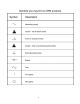
TABLE OF CONTENTS Condensed Information SAFETY and Preparation for use Symbols Specifications Front Panel Summary Abridged Command List Status Byte Definition Configuration Switches Guide to Operation Front Panel Signal Inputs Signal Filters Sensitivity Dynamic Reserve Status Indicators Display Select Output Expand Function Rel Function Offset Time Constants Noise Measurements Reference Input and Trigger Levels Phase Controls Power Switch Local/Remote Operation Default Settings 1 2 3 5 6 7 7 8 8 8 8 9 9 9
RS232 Interface GPIB Interface Power Supplies Internal Oscillator 32 32 33 33 Calibration and Repair Introduction Multiplier Adjustments Amplifier and Filter Adjustments CMRR Adjustment Line Notch Filter Adjustment 2xLine Notch Filter Adjustment Repairing Damaged Front-End 34 34 34 34 35 35 35 Appendix A: Noise Sources and Cures Johnson Noise '1/f' Noise Noise Spectrum Capacitive Coupling Inductive Coupling Ground Loops Microphonics Thermocouple Effect 36 36 36 37 37 38 38 38 Appendix B: RS232 Simples
Safety and Preparation for Use ***CAUTION***: This instrument may be damaged if operated with the LINE VOLTAGE SELECTOR set for the wrong applied ac input-source voltage or if the wrong fuse is installed. LINE VOLTAGE SELECTION OPERATE WITH COVERS IN PLACE The SR510 operates from a 100V, 120V, 220V, or 240V nominal ac power source having a line frequency of 50 or 60 Hz.
2
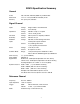
SR510 Specification Summary General Power Mechanical Warranty 100, 120, 220, 240 VAC (50/60 Hz); 35 Watts Max 17" x 17" x 3.5" (Rack Mount Included) 12 lbs. Two years parts and labor. Signal Channel Inputs Voltage: Current: Single-ended or True Differential 106 Volts/Amp Impedance Voltage: 100 MΩ + 25 pF, ac coupled Full Scale Current: Voltage: 1 kΩ to virtual ground 100 nV (10 nV on expand) to 500 mV Current: Voltage: 100 fA to 0.
Acquisition Time Slew Rate Phase Control Phase Noise Phase Drift Phase Error 25 Sec at 1 Hz 6 Sec at 10 Hz 2 Sec at 10 kHz 1 decade per 10 S at 1 kHz 90° shifts Fine shifts in 0.025° steps 0.01° rms at 1 kHz, 100 msec, 12 dB TC 0.1°/°C Less than 1° above 10Hz Demodulator Stability Time Constants Offset Harmonic Rej 5 ppm/°C on LOW dynamic reserve 50 ppm/°C on NORM dynamic reserve 500 ppm/°C on HIGH dynamic reserve Pre: 1msec to 100 sec (6 dB/Octave) Post: 1sec, 0.
Front Panel Summary Signal Inputs Single Ended (A), True Differential (A-B), or Current (I) Signal Filters Bandpass: Q-of-5 Auto-tracking filter (In or Out) Line Notch: Q-of-10 Notch Filter at line frequency (In or Out) 2XLine Notch: Q-of-10 Notch Filter at twice line frequency (In or Out) Sensitivity Full scale sensitivity from 100 nV to 500 mV RMS for voltage inputs or from 100 fA to 500 nA RMS for current inputs.
Abridged Command List A A0 A1 Return the ‘REL’ Status Turn the ‘REL’ off Turn the ‘REL’ on B B0 B1 Return Bandpass Filter Status Take out the Bandpass Filter Put in the Bandpass Filter C C0 C1 Return the Reference LCD Status Display the Reference Frequency Display the Reference Phase Shift D D0 D1 D2 Return Dynamic Reserve Setting Set DR to LOW range Set DR to NORM range Set DR to HIGH range En En,0 En,1 Return Expand Status Turn Expand off Turn Expand on F Return the Reference Frequency G G1 ..
Status Byte Definition Bit Meaning 0 Magnitude too small to calculate phase 1 Command Parameter is out-of-range 2 No detectable reference input 3 PLL is not locked to the reference 4 Signal Overload 5 Auto-offset failed: signal too large 6 SRQ generated 7 Unrecognized or illegal command Configuration Switches There are two banks of 8 switches, SW1 and SW2, located on the rear panel. SW1 sets the GPIB address and SW2 sets the RS232 parameters.
allowable signals at the inputs. The notch frequencies are set at the factory to either 50 Hz or 60 Hz. The user can adjust these frequencies. (See the Maintenance and Repair section for alignment details.) These filters precede the bandpass filter in the signal amplifier. SR510 Guide to Operation Front Panel The front panel has been designed to be almost self-explanatory.
Dynamic Reserve Sensitivity Range LOW NORM HIGH 1 µV through 500 mV 100 nV through 50 mV 100 nV through 5 mV REM indicates that the unit is in the remote state and that the front panel controls are not operative. There are two remote states. The Remote-WithLockout will not allow any inputs from the front panel. The Remote-Without-Lockout command allows you to return the front panel to operation by pressing the DISPLAY UP key.
currently displayed parameter. If the output is greater than 1.024 times full scale, the REL function will not be able to zero the output and the ON LED will blink. The offset value will then be set to its max value. If NOISE is being displayed when the REL function is turned on, the noise ouptut will require a sew seconds to settle again. Vout = 10Ae(AvVicosØ+Vos) where...
only by the ac 'wiggles' at the output. By measuring the noise at different frequencies, the frequency dependence of the noise density can be found. This usually has the form of vnoise ~ 1/f. The noise computation assumes that the noise has a Gaussian distribution (such as Johnson noise). Since the computation takes many time constants (reciprocal bandwidth), the noise output should be allowed to approach a steady value before a reading is taken.
whenever any of the PHASE keys are pressed. The phase ranges from -180 degrees to +180 degrees and is the phase delay from the reference input signal. Defaults If the REL key is held down when the POWER is turned on, the instrument settings will be set to the defaults shown below instead of the settings in effect when the power was turned off. Power This is the instrument's POWER switch.
SR510 Guide to Operation Rear Panel AC Power The ac line voltage selector card, line fuse, and line cord receptacle are located in the fuse holder at the left side of the rear panel. See the section, Preparation for Use at the front of this manual for instructions on setting the ac voltage selector and choosing the correct fuse.
OUTPUT can be set to three amplitudes, 1 V, 100 mV, and 10 mV (rms) using the amplitude switch. The output impedance is 600Ω. The AMP CAL screw adjusts the amplitude. 2) If the VCO INPUT is left open, then the oscillator will run at the top of its range (i.e. 10 Hz, 1 KHz, or 100 KHz). 3) A 10 KΩ potentiometer may be connected from the VCO INPUT to ground. This pot will then set the frequency. The oscillator frequency is controlled by the VCO INPUT voltage.
SR510 Guide to Programming An example of a multiple command is: G 5; T 1,4; P 45.10 It is not necessary to wait between commands. The SR510 has a command input buffer of 256 characters and processes the commands in the order received. Likewise, the SR510 has an output buffer (for each interface) of 256 characters. The SR510 Lock-in Amplifier is remotely programmable via both RS232 and GPIB interfaces. It may be used with laboratory computers or simply with a terminal.
The REM LED is on whenever the SR510 is programmed to be in the remote state. to the terminal. Now read the gain using the sensitivity read command, G. The response should be 24 meaning that the sensitivity is at the 24th setting or 500 mV. Change the sensitivity by typing G19. The sensitivity should now be 10 mV. Check the front panel to make sure this is so.
F The F command reads the reference frequency. For example, if the reference frequency is 100 Hz, the F command returns the string "100.0". If the reference frequency is 100.0 kHz, the string "100.0E+3" is returned. The F command is a read only command. SR510 Command List The first letter in each command sequence is the command. The rest of the sequence consists of parameters. Multiple parameters are separated by a comma. Those parameters shown in {} are optional while those without {} are required.
n Status 0 Local: all front panel keys are operative 1 Remote: front panel keys are not operative. The display up key returns the status to local. 2 Lock-out: front panel keys are not operative. No key returns the status to local. Another I command is needed to return to local. 20 21 22 23 24 25 26 27 L m {,n} The L command sets and reads the status of the line notch filters. If m is "1", then the 1X line notch is selected, if m is "2", the 2X line notch is selected. The parameter m is required.
Q The Q command returns the output reading in units of volts. For an input signal of 50 µV on a full scale sensitivity of 100 µV, the Q command will return the string "50.00E-6". The parameter read is the same as that being shown on the output display and can be changed with the S command. U m {,n} The U command sets and reads the unit's ROM calibration bytes. m is the address offset of the byte, 0-255. If n is absent, the value of the addressed calibration byte is returned.
Overload. This bit is set if there is a signal overload. This can happen when the sensitivity is too high, the dynamic reserve is too low, the offset is on, or the expand is on. Overloads on the general purpose A/D inputs or the ratio output are not detected. LED will be on for about 2 seconds to indicate that the stored instrument settings are being ignored. If the RS232 echo mode is on, the sign-on message is sent over the RS232 interface. Status Byte Bit 5 Auto Offset Out of Range.
seen Microsoft's Interpreted Basic on the IBM PC occasionally send a curly bracket (ASCII 253) when it was supposed to have sent a carriage return (ASCII 13). Trouble-Shooting Interface Problems 2) Your computer's baud rate has been changed and no longer matches the SR510's baud rate. If you are having difficulty getting your computer to communicate with the SR510 look to the sections on the RS232 and GPIB interfaces for some tips specific to your particular interface.
Up to four terminating characters may be specified by the J command. If no arguments are sent with the J command, the terminating sequence returns to the default (echo on: ; echo off: ). Data Communications Equipment (DCE) The SR510 is configured as DCE so that it may be connected directly to a terminal. If the SR510 is to be interfaced with another DCE device, a special cable (sometimes referred to as a 'modem' cable) is required.
the RS232 interface has no provision for bus commands and remote commands over the RS232 interface would never be enabled. GPIB with RS232 Echo Mode It is sometimes useful when debugging a GPIB system to have some way of monitoring exactly what is going back and forth over the bus. The SR510 has the capability to echo all characters sent and received over the GPIB to its RS232 port. This mode of operation is enabled by setting switch 6 of SW1 to the DOWN position.
The Lock-in Technique A Measurement Example The Lock-in technique is used to detect and measure very small ac signals. A Lock-in amplifier can make accurate measurements of small signals even when the signals are obscured by noise sources which may be a thousand times larger. Essentially, a lock-in is a filter with an arbitrarily narrow bandwidth which is tuned to the frequency of the signal. Such a filter will reject most unwanted noise to allow the signal to be measured.
Vpsd = cos(wr+Ø) cos(wst) = 1/2 cos[(wr + ws)t+Ø] + 1/2 cos[(wr - ws)t+Ø] single pole filter is 1/4RC. The output will converge exponentially to the final value with a 10 second time constant. If we wait 50 seconds, the output will have come to within 0.7% of its final value. The dynamic reserve of 60 dB is required by our expectation that the noise will be a thousand times larger than the signal. Additional dynamic reserve is available by using the bandpass and notch filters.
(as is the case here) the noise picked up by the shield will also appear on the center conductor. This is good, because the lock-in's 100 dB CMRR will reject most of this common mode noise. However, not all of the noise can be rejected, especially the high frequency noise, and so the lock-in may overload on the high sensitivity ranges.
bandpass filter adds a few nanovolts of noise to the front end of the instrument when it is in use. In many servo applications, no output filtering is needed. In this case, the SR510 may be modified to reduce the output time constant to about 20 µS. Contact the factory for details. Line Notch Filters should be used in most measurement situations. The filters will reject about 50 dB of line frequency noise (about a factor of 300).
SR510 Block Diagram Several new concepts are used to simplify the design of SR510 lock-in amplifier. In addition to implementing recent advances in linear integrated circuit technology, the instrument was designed to take full advantage of its microprocessor controller to improve performance and to reduce cost. some noise source, giving a spurious result. To overcome this difficulty designers employed tuned amplifiers or heterodyning techniques.
instrument. The output is most stable when most of the gain is in the ac amplifier, however, high ac gain reduces the dynamic reserve. The Signal Channel The instrument has both current and voltage inputs. The current input is a virtual ground, and the 100 MΩ voltage inputs can be used as singleended or true differential inputs. For the most demanding applications, the user may specify how the system gain is partitioned.
Circuit Description between the two transistors and therefore their gain match and common mode rejection. Introduction The output of the pre-amp is scaled by resistors R119-R122 and analog switch U103 which make up a 1-2-5-10 attenuator. The signal is then amplified by 2/2 U102. Input overload is sensed through diodes D101-D104. The SR510 Lock-in amplifier is an integrated instrument combining state of the art analog design with advanced microprocessor based control and interfaces.
The triangle output is divided by R363 and R362 before reaching transconductance amplifier 2/2 U322. The amplitude of the triangle input to this amplifier is enough to just saturate the input and provide a sine wave output. 2/2 U325 then amplifies the sine wave before it goes to the demodulator. U324 is a comparator which generates a square wave in-phase with the sine output. U326 divides the frequency of the square wave by 8 and 2/2 U327 selects the frequency of the square wave chopper.
is sampled and held on capacitor C502 and buffered by 4/4 U508. The A/D conversion is done by successive approximation using comparator U514 to compare the sampled and held signal with known outputs of U505, a 12 bit DAC with a precision reference. Note that the output of U506, an 8 bit DAC is summed with the output of U505. This 8 bit DAC corrects for offset errors which can accumulate as analog voltages pass through buffers, S/H amps, and comparators.
whenever a GPIB transaction occurs which requires the CPU’s response. (The GPIB address is set by switch bank SW1.) Internal Oscillator The internal oscillator is on a small circuit board attached to the rear panel of the instrument. Local regulators, Q1 and Q2, provide power to the board. The VCO input is internally pulled up by R12. This pulls the VCO input to 10V when the VCO input is left open. 2/4 U1 translates the VCO input voltage to provide a negative control voltage to U2, the function generator.
Calibration and Repair This section details calibration of the instrument. Calibration should only be done by a qualified electronics technician. ********** WARNING ********** The calibration procedure requires adjusting the instrument with power applied and so there is a risk of personal injury or death by electric shock. Please be careful. Most of the calibration parameters are determined by a computer aided calibration procedure after burn-in at the factory.
Notch Filters Replacing the Front-End Transistors Set the reference frequency to 60.0 Hz (50.0 Hz). It is convenient to use the SYNC output of the signal generator as the reference input if it is available. Connect the sine output of the signal generator to the A input and set the input selector to A. With the SENSITIVITY at 100mV, adjust the amplitude of the input signal to 100 mV (full scale). Both the voltage and current front end transistors (Q101 and Q102) are 2N6485 (IMF6485) dual JFETS.
Appendix A: Noise Sources and Cures And Others. Other noise sources include flicker noise found in vacuum tubes, and generation and recombination noise found in semiconductors. Noise, random and uncorrelated fluctuations of electronic signals, finds its way into experiments in a variety of ways. Good laboratory practice can reduce noise sources to a manageable level, and the lock-in technique can be used to recover signals which may still be buried in noise.
Capacitive Coupling. A voltage on a nearby piece of apparatus (or operator) can couple to a detector via a stray capacitance. Although Cstray may be very small, the coupled in noise may still be larger than a weak experimental signal. Inductive Coupling. Here noise couples to the experiment via a magnetic field: Inductive Noise Coupling A changing current in a nearby circuit gives rise to a changing magnetic field which induces an emf in the loop connecting the detector to the experiment. (emf = dØB/dt.
Resistive Coupling (or 'Ground Loops'). Currents through common connections can give rise to noise voltages. Microphonics provides a path for mechanical noise to appear as electrical noise in a circuit or experiment. Consider the simple circuit below: The capacitance of a coaxial cable is a function of its geometry so mechanical vibrations will cause the cable capacitance to vary with time.
the terminal responds to a control line, it will believe that the SR510 is not ready to accept data (because the line is not passed in this example) and will therefore not send any data. Appendix B: Introduction to the RS232 The 'RS232' is a standard for bit serial asynchronous data communication. The standard defines the format for data transmission, the electrical specifications for the signal levels, and the mechanical dimensions of connectors. CASE 2 - RS232 with Control Lines.
transmitted (11bits/19.2K baud.) The typical data string 5.1270 has 7 characters, requiring 4 msec to be sent. If a parity option was selected, the parity bit would be sent after the 8th data bit, but before the first stop bit. Stop Bits Final Tip Generally, selection of 2 stop bits will result in fewer data transmission errors.
Data Bus: There are eight data lines which use negative logic and pass the bits of each byte in parallel. Appendix C: Introduction to the GPIB General Interface Lines: These five lines operate independently of the handshake lines and use negative logic. The IEEE-488 Standard specifies the voltage levels, handshake requirements, timing, hardware details, pinout and connector dimensions for a 16 line, bit parallel bus. Many instruments may be connected in series to communicate over the same cable.
Appendix D: Program Examples All of the program examples which follow do the same thing, only the computer, language, or interface is changed. The programs read the Channel 1 and 2 Outputs and write the results to the computer screen. In addition, the X6 analog output port is ramped from 0 to 10V. Program Example 1: IBM PC, Basic, via RS232 In this example, the IBM PC's ASYNC port (known as COM1: or AUX: to DOS users) will be used to communicate with the SR510.
Program Example 2: IBM PC, Microsoft Fortran v3.3, via RS232 Machine language routines to interface to the COM1: RS232 port are provided in the file RS232.OBJ found on the SR575 disk. These routines allow for simple interfacing to the SR510 at 19.2 kbaud from FORTRAN programs. To use these routines, the file 'for232.inc' (also on the SR575 disk) must be 'included' in the FORTRAN source.
[ 2000 print results to screen write(*,2000) v1 format(′ Output 1=′,G10.3) [ ramp x6 by 2.5 mV x6 = x6 + .0025 if (x6.gt.10) x6 = 0.0 [ make x6 command string write (str2,3000) x6 format (′x6,′,f7.3,′$′) call txstr(str2) 3000 [ and loop forever goto 20 stop end [ *********************************** subroutine nocom [ [ in case of a timeout error, this routine runs put your error handler here.
Program Example 3: IBM PC, Microsoft C v3.0, via RS232 Machine language routines to interface to the COM1: RS232 port are provided in the file RS232.OBJ found on the SR565 disk. These routines allow for simple interfacing to the SR510 at 19.2 kbaud from C programs. To use these routines, the large model must be used. Compile with the /AL switch and link with RS232.OBJ.
x += 0.0025; /* increment x6 output by 2.5 mV */ if (x >= 10) x = 0; sprintf (str2, ″X6,%f$″, x); /* make x6 command string */ txstr (str2); /* send x6 command */ /* print results to screen */ printf (″Output = %10.
Program Example 4: IBM PC,Microsoft Basic, via GPIB This program requires the Capital Equipment Corporation GPIB card for the IBM PC or XT. It has firmware in ROM to interface high level languages to the GPIB. In this program, the CEC card's ROM starts at OC0000H, the system controller's address is 21, and the SR530 has been assigned as GPIB address 23. Subroutine calls in Microsoft BASIC are done to memory locations specified by the name of the subroutine.
390 400 410 420 430 440 450 460 470 480 490 500 510 520 530 540 550 560 CALL TRANSMIT (X$,STATUS%) ′SET NEW X6 VOLTAGE GOSUB 540 ′ GOTO 280 ′LOOP FOREVER ′ ′ GET AN ANSWER STRING FROM THE SR510 CALL TRANSMIT(LISN$,STATUS%) ′MAKE SR510 A TALKER GOSUB 540 ANS$=SPACE$(10) ′INIT ANSWER STRING CALL RECV(ANS$,LENGTH%STATUS%) ′READ RESULT INTO ANS$ GOSUB 540 RETURN ′ ′ ′ CHECK STATUS OF LAST TRANSMISSION FOR ERRORS IF STATUS%=0 THEN RETURN ′STATUS OKAY PRINT ″STATUS CODE = ″;STATUS%;″ ON GPIB: ERROR″ STOP 48
Program Example 5: HP85 via GPIB This program provides an example of an HP85 program using the GPIB interface which could be used to control the lockin amplifier. In this example, the SR510 should be addressed as device #16 by setting the switch bank SW1 per the instructions Page 7. 10 20 30 40 50 60 70 80 x=0 OUTPUT 716 ; ″Q″ ENTER 716 : V1 DISP ″OUTPUT = ″ : V1 X = X + .
Documentation This section contains the parts lists and schematics for the SR510 lock-in amplifier. The first digit of any part number can be used to locate the scematic diagram for the part. For example, R415 is located on sheet 4 of the schematic diagrams.
SR510 PARTS LIST Main Assembly PCB Parts List NO 1. 2. 3. 4. 5. 6. 7. 8. 9. 10. 11. 12. 13. 14. 15. 16. 17. 18. 19. 20. 21. 22. 23. 24. 25. 26. 27. 28. 29. 30. 31. 32. 33. 34. 35. 36. 37. 38. 39. 40. 41. 42. 43. 44. 45. 46. 47. 48. 49. REF.
SR510 PARTS LIST NO 50. 51. 52. 53. 54. 55. 56. 57. 58. 59. 60. 61. 62. 63. 64. 65. 66. 67. 68. 69. 70. 71. 72. 73. 74. 75. 76. 77. 78. 79. 80. 81. 82. 83. 84. 85. 86. 87. 88. 89. 90. 91. 92. 93. 94. 95. 96. 97. 98. 99. 100. REF.
SR510 PARTS LIST NO 101. 102. 103. 104. 105. 106. 107. 108. 109. 110. 111. 112. 113. 114. 115. 116. 117. 118. 119. 120. 121. 122. 123. 124. 125. 126. 127. 128. 129. 130. 131. 132. 133. 134. 135. 136. 137. 138. 139. 140. 141. 142. 143. 144. 145. 146. 147. 148. 149. 150. 151. REF.
SR510 PARTS LIST NO 152. 153. 154. 155. 156. 157. 158. 159. 160. 161. 162. 163. 164. 165. 166. 167. 168. 169. 170. 171. 172. 173. 174. 175. 176. 177. 178. 179. 180. 181. 182. 183. 184. 185. 186. 187. 188. 189. 190. 191. 192. 193. 194. 195. 196. 197. 198. 199. 200. 201. 202. REF.
SR510 PARTS LIST NO 203. 204. 205. 206. 207. 208. 209. 210. 211. 212. 213. 214. 215. 216. 217. 218. 219. 220. 221. 222. 223. 224. 225. 226. 227. 228. 229. 230. 231. 232. 233. 234. 235. 236. 237. 238. 239. 240. 241. 242. 243. 244. 245. 246. 247. 248. 249. 250. 251. 252. 253. REF.
SR510 PARTS LIST NO 254. 255. 256. 257. 258. 259. 260. 261. 262. 263 264. 265. 266. 267. 268. 269. 270. 271. 272. 273. 274. 275. 276. 277. 278. 279. 280. 281. 282. 283. 284. 285. 286. 287. 288. 289. 290. 291. 292. 293. 294. 295. 296. 297. 298. 299. 300. 301. 302. 303. 304. REF.
SR510 PARTS LIST NO 305. 306. 307. 308. 309. 310. 311. 312. 313. 314. 315. 316. 317. 318. 319. 320. 321. 322. 323. 324. 325. 326. 327. 328. 329. 330. 331. 332. 333. 334. 335. 336. 337. 338. 339. 340. 341. 342. 343. 344. 345. 346. 347. 348. 349. 350. 351. 352. 353. 354. 355. REF.
SR510 PARTS LIST NO 356. 357. 358. 359. 360. 361. 362. 363. 364. 365. 366. 367. 368. 369. 370. 371. 372. 373. 374. 375. 376. 377. 378. 379. 380. 381. 382. 383. 384. 385. 386. 387. 388. 389. 390. 391. 392. 393. 394. 395. 396. 397. 398. 399. 400. 401. 402. 403. 404. 405. 406. REF.
SR510 PARTS LIST NO 407. 408. 409. 410. 411. 412. 413. 414. 415. 416. 417. 418. 419. 420. 421. 422. 423. 424. 425. 426. 427. 428. 429. 430. 431. 432. 433. 434. 435. 436. 437. 438. 439. 440. 441. 442. 443. 444. 445. 446. 447. 448. 449. 450. 451. 452. 453. 454. 455. 456. 457. REF.
SR510 PARTS LIST NO 458. 459. 460. 461. 462. 463. 464. 465. 466. 467. 468. 469. 470. 471. 472. 473. 474. 475. 476. 477. 478. 479. 480. 481. 482. 483. 484. 485. 486. 487. 488. 489. 490. 491. 492. 493. 494. 495. 496. 497. 498. 499. 500. 501. 502. 503. 504. 505. 506. 507. 508. REF.
SR510 PARTS LIST NO 509. 510. 511. 512. 513. 514. 515. 516. 517. 518. 519. 520. 521. 522. 523. 524. 525. 526. 527. 528. 529. 530. 531. 532. 533. 534. 535. 536. 537. 538. 539. 540. 541. 542. 543. 544. 545. 546. 547. 548. 549. 550. 551. 552. 553. 554. 555. 556. 557. 558. 559. REF.
SR510 PARTS LIST NO 560. 561. 562. 563. 564. 565. 566. 567. 568. 569. 570. 571. 572. 573. 574. 575. 576. 577. 578. 579. 580. 581. 582. 583. 584. 585. 586. 587. 588. 589. 590. 591. 592. 593. 594. 595. 596. 597. 598. 599. 600. 601. 602. 603. 604. 605. 606. 607. 608. 609. 610. REF.
SR510 PARTS LIST NO 611. 612. 613. 614. 615. 616. 617. 618. 619. 620. 621. 622. 623. 624. 625. 626. 627. 628. 629. 630. 631. 632. 633. 634. 635. 636. 637. 638. 639. 640. 641. 642. 643. 644. 645. 646. 647. 648. 649. 650. 651. 652. 653. 654. 655. 656. 657. 658. 659. 660. 661. REF.
SR510 PARTS LIST No 662. 663. 664. 665. 666. 667. 668. 669. 670. 671. 672. 673. 674. 675. 676. 677. 678. 679. 680. 681. 682. 683. 684. 685. 686. 687. 688. 689. 690. 691. 692. 693. 694. 695. 696. 697. 698. 699. 700. 701. 702. 703. 704. 705. 706. 707. 708. 709. 710. 711. 712. REF.
SR510 PARTS LIST NO 713. 714. 715. 716. 717. 718. 719. 720. 721. 722. 723. 724. 725. 726. 727. 728. 729. REF.
SR510 PARTS LIST NO 30. 31. 32. 33. 34. 35. 36. 37. 38. 39. 40. 41. 42. 43. 44. 45. 46. 47. 48. 49. REF. R 15 R 16 R 17 R 18 R 19 R 20 R 21 R 22 R 23 R 24 R 25 SW1 SW2 U1 U2 U3 U4 Z0 Z0 Z0 SRS part# 4-00022-401 4-00079-401 4-00104-401 4-00034-401 4-00034-401 4-00188-407 4-00188-407 4-00022-401 4-00022-401 4-00031-401 4-00031-401 2-00013-215 2-00013-215 3-00087-340 3-00085-340 3-00118-325 3-00124-325 0-00100-040 0-00122-053 0-00136-053 VALUE 1.0M 4.7K 82K 10K 10K 4.99K 4.99K 1.0M 1.
SR510 PARTS LIST Front Panel Parts List NO 1. 2. 3. 4. 5. 6. 7. 8. 9. 10. 11. 12. 13. 14. 15. 16. 17. 18. 19. 20. 21. 22. 23. 24. 25. 26. 27. 28. 29. 30. 31. 32. 33. 34. 35. 36. 37. 38. 39. 40. 41. 42. 43. 44. 45. 46. 47. 48. 49. REF.
SR510 PARTS LIST NO 50. 51. 52. 53. 54. 55. 56. 57. 58. 59. 60. 61. 62. 63. 64. 65. 66. 67. 68. 69. 70. 71. 72. 73. 74. 75. 76. 77. 78. 79. 80. 81. 82. 83. 84. 85. 86. 87. 88. 89. 90. 91. 92. 93. 94. 95. 96. 97. 98. 99. 100. REF.
SR510 PARTS LIST NO 101. 102. 103. 104. 105. 106. 107. 108. 109. 110. 111. 112. 113. 114. 115. 116. 117. 118. 119. 120. 121. 122. 123. 124. 125. 126. 127. 128. 129. 130. 131. 132. 133. 134. 135. 136. 137. 138. 139. 140. 141. 142. REF.