
User's Manual
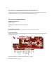


N4 is general purpose medium-power switches in telecommunication applications and suitable for 2.4GHz
design. C35 and C40 are blocking capacitors required by N4. L1 and C3 are 50 ohm impedance tuning
components for chip antenna. Between J5 and C35 is 50ohm microstrip refer to layer2. D3 is for ESD
protection. J5 is a i-pex connector. The external omni antenna is connected to J5 by MHF-to-SMA cable.
The following conditions are required for MHF-to-SMA cable connected to J5.
a. Frequency range: DC -3GHz
b. Impedance: 50ohm
c. VSWR: 1.5(max)
5 RF exposure considerations
The host device manufacturer should confirm that a separation distance of 20 cm or more should be
maintained between the antenna of this host device and persons during the host device operation.
6 Antennas
For 2.4G Band:
Ant1: Internal chip antenna, 4dBi;
Ant2: External omni antenna, 3dBi;
7 Label and compliance information
If this certified module is installed inside the host device, then the outside of the host must be labeled
with “Contains FCC ID: 2AXNQ2101A and IC: 27995-2101A”.
8 Information on test modes and additional testing requirements
The host manufacturer can use software to make transmit continuously.
9 Additional testing, Part 15 Subpart B disclaimer
The module only complies with the FCC Part 15.247. If the module is installed in the host device, the host
manufacturer is responsible for the compliance to any other FCC rules that apply to the host not covered
by the modular transmitter grant of certification. For example, if the host manufacturer markets their
product as being Part 15 Subpart B compliant (when it also contains unintentional-radiator digital circuity),
then the host manufacturer shall provide a notice stating that the final host product still requires Part 15
Subpart B compliance testing with the modular transmitter installed.