
User's Manual


Doc ID TBD Rev 0.8 Rev 0.1
11/19
www.st.com
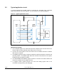
3.3 Layout guidelines
The application PCB requires a flooded ground plane. Care must be taken to ensure
there are no traces or ground planes under the area surrounding the antenna, with the
exception of minimal width traces from pins 1,2,3,4,13,14,15 and 16 of the module if these
are used. It is appropriate to place the module toward the edge of the PCB with no traces
or ground planes from the antenna to the board edge.
Figure 4. Layout guidelines
Application PCB
No copper on any layer surrounding antenna, except
minimal traces from pins 1,2,3,4,13,14,15 and 16
Flooded ground plane required
(signal traces allowed)
min .
6 mm
min .
6 mm