
User's Manual
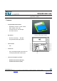
SP
SGRF
Rev 1.0 P a g e | 7
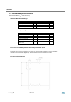
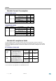
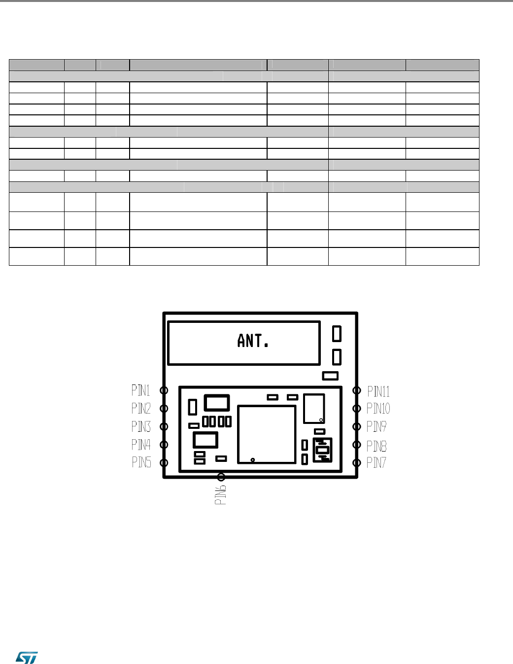
Pin Assignment
Name Type Pin # Description
ALT Function
V
max.
Tolerant
Initial State
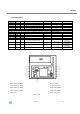
SPI Interface
SPI_CLK I 7
SPI CLOCK (Max. 8 MHz)
V
in
SPI_MOSI I 9
SPI MOSI (MASTER out SLAVE in)
V
in
SPI_MISO O 8
SPI MISO (MASTER in / SLAVE out)
V
in
SPI_CS I 10
SPI “Chip Select” (SPI slave select)
V
in
Power and Ground
V
in
5
V
in
(1.8V + 3.6V max.)
GND 6
GND
Module SHUTDOWN
SDN I 11
SHUTDOWN input (active high.)
(1.8V + V
in
max).
GPIO – General Purpose Input/Output
GPIO [0] I/O 4
Programmable Input / Output
& Analog Temperature output
(1.8V + V
in
max.).
Digital Output
.
Low Power
GPIO [1] I/O 3
Programmable Input / Output
(1.8V + V
in
max.).
Digital Output
.
Low Power
GPIO [2] I/O 2
Programmable Input / Output
(1.8V + V
in
max.).
Digital Output
.
Low Power
GPIO [3] I/O 1
Programmable Input / Output
(1.8V + V
in
max.).
Digital Output
.
Low Power
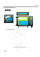
Pin1 = GPIO_3 (TBD) Pin11 = SDN
Pin2 = GPIO_2 (TBD) Pin10 = SPI_CS
Pin3 = GPIO_1 (TBD) Pin9 = SPI_MOSI
Pin4 = GPIO_0 (TBD) Pin8 = SPI_MISO
Pin5 = Vin Pin7 = SPI_CLK
Pin6 = GND