
User's Manual

Rev 0.1 P a g e | 7
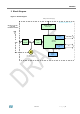
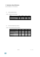
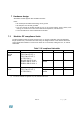
5.4 Pin Assignement
Figure 3 – Pin connection diagram
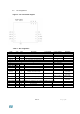
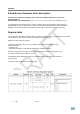
Table 6 – Pin Assignment
Name
Type
Pin #
Description
ALT Function
V max. Tolerant
Initial State
SPI Interface
SPI_CLK
I
7
SPI CLOCK (Max. 8 MHz)
V
in
SPI_MISO
O
8
SPI MISO (MASTER in / SLAVE out)
V
in
SPI_MOSI
I
9
SPI MOSI (MASTER out SLAVE in)
V
in
SPI_CS
I
10
SPI “Chip Select” (SPI slave select)
V
in
Power and Ground
V
in
5
V
in
(1.8V + 3.6V max.)
GND
6
GND
Module SHUTDOWN
SDN
I
11
SHUTDOWN input (active high)
(1.8V + 3.6V max.).
GPIO – General Purpose Input/Output
GPIO [0]
I/O
4
Programmable Input / Output
& Analog Temperature output
(1.8V + V
in
max.).
Digital Output.
Low Power
GPIO [1]
I/O
3
Programmable Input / Output
(1.8V + V
in
max.).
Digital Output.
Low Power
GPIO [2]
I/O
2
Programmable Input / Output
(1.8V + V
in
max.).
Digital Output.
Low Power
GPIO [3]
I/O
1
Programmable Input / Output
(1.8V + V
in
max.).
Digital Output.
Low Power
Optional External Antenna connections (Not available on the standard SPSGRFC-xxx modules)
N.C.
N.C
12
Not connected
N.C.
N.C.
13
Not connected
N.C.
N.C.
14
Not connected