
User's Manual


SPZB260C-PRO / SPZB260A-PRO
5/10
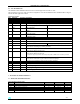
3.2 - RECOMMENDED OPERATING CONDITIONS
Table 3. Recommended operating conditions
Symbol Parameter Conditions Min Typ Max Unit
VDD Module supply voltage -40°C < T < 85°C 2.1 3.3 3.6 V
Tstg Operating ambient temperature -40 +85 °C
4 - ELECTRICAL CHARACTERISTICS
4.1 – DC ELECTRICAL CHARACTERISTICS
Tabl4. DC Electrical Characteristics
Symbol Parameter Conditions Min Typ Max Unit
IRX RX current ( boost mode) Vdd = 3.0 V T= 25 °C 38 mA
IRX RX current ( normal mode) Vdd = 3.0 V T= 25 °C 36 mA
ITX TX current ( boost mode) Vdd = 3.0 V T= 25 °C
42 mA
ITX TX current (normal mode) Vdd = 3.0 V T= 25 °C
36 mA
IDS Deep Sleep Current 2.1 < Vdd < 3.6 V
T = 25°C
1
µΑ
4.2 - DIGITAL I/O SPECIFICATIONS
Table5. Digital I/O Specifications
Symbol Parameter Conditions Min Typ Max Unit
VIL Low Level Input Voltage 2.1 < Vdd < 3.6 V 0 0.2 x
Vdd
V
VIH High level input voltage 2.1 < Vdd < 3.6 V 0.8 x Vdd Vdd V
Iil Input current for logic 0 2.1 < Vdd < 3.6 V -0.5
µΑ
Iih Input current for logic 1 2.1 < Vdd < 3.6 V 0.5
µΑ
Ripu Input pull-up resistor 30
κΩ
Ripd Input pull-down resistor 30
κΩ
VOL Low level output voltage 0 0.18 x
Vdd
V
VOH High level output voltage 0.82 x Vdd Vdd V
IOHS Output source current
(standard pin)
4 mA
IOLS Output sink current
(standard pin)
4 mA
IOHH Output source current (pin 17,18,19 ) 8 mA
IOLH Output sink current (pin 17,18,19 ) 8 mA
IOTot Total output current for I/O pins 40 mA
4.3 - RF ELECTRICAL CHARACTERISTICS
Table6. RF Electrical Characteristics (with UFL connector )
Symbol Parameter Conditions Min Typ Max Unit
Frequency range 2.1 < Vdd < 3.6 V 2405 2480 MHz
TX Output power Vdd = 3.0V F= 2450 Mhz 3 dBm
RX Sensitivity Vdd = 3.0V 1% PER -95 dBm
Carrier frequency error Vdd=3.0V -20 / + 70 °C
-40 40 ppm