L78S00 SERIES 2A POSITIVE VOLTAGE REGULATORS ■ ■ ■ ■ ■ OUTPUT CURRENT TO 2A OUTPUT VOLTAGES OF 5; 7.5; 9; 10; 12; 15; 18; 24V THERMAL OVERLOAD PROTECTION SHORT CIRCUIT PROTECTION OUTPUT TRANSITION SOA PROTECTION DESCRIPTION The L78S00 series of three-terminal positive regulators is available in TO-220 and TO-3 packages and with several fixed output voltages, making it useful in a wide range of applications.
L78S00 SERIES ABSOLUTE MAXIMUM RATINGS Symbol VI Parameter² DC Input Voltage Value for VO = 5 to 18 V 35 for VO = 24 V 40 Unit V Output Current Internally Limited Ptot Power Dissipation Internally Limited Tstg Storage Temperature Range -65 to 150 °C Top Operating Junction Temperature for L78S00 Range for L78S00C -55 to 150 0 to 150 °C IO Absolute Maximum Ratings are those values beyond which damage to the device may occur. Functional operation under these condition is not implied.
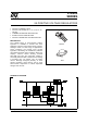
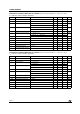
L78S00 SERIES CONNECTION DIAGRAM (top view) TO-220 TO-3 ORDERING CODES TYPE L78S05 L78S05C L78S75 L78S75C L78S09 L78S09C L78S10 L78S10C L78S12 L78S12C L78S15 L78S15C L78S18 L78S18C L78S24 L78S24C TO-220 L78S05CV L78S75CV L78S09CV L78S10CV L78S12CV L78S15CV L78S18CV L78S24CV TO-3 OUTPUT VOLTAGE L78S05T L78S05CT L78S75T L78S75CT L78S09T L78S09CT L78S10T L78S10CT L78S12T L78S12CT L78S15T L78S15CT L78S18T L78S18CT L78S24T L78S24CT 5V 5V 7.5 V 7.
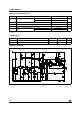
L78S00 SERIES TEST CIRCUITS Figure 1 : DC Parameters Figure 2 : Load Regulation Figure 3 : Ripple Rejection 4/24
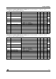
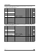
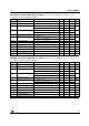
L78S00 SERIES ELECTRICAL CHARACTERISTICS OF L78S05 (refer to the test circuits, TJ = 25°C, VI = 10 V, IO = 500 mA, unless otherwise specified). Symbol Parameter Test Conditions VO Output Voltage VO Output Voltage IO = 1 A ∆VO Line Regulation VI = 7 to 25 V ∆VO Load Regulation Id ∆Id eN Typ. Quiescent Current Change Max. Unit 4.8 5 5.2 V 4.75 5 5.25 V 100 mV VI = 8 to 25 V 50 IO = 20 mA to 2 A 100 8 mA IO = 20 mA to 1 A 0.
L78S00 SERIES ELECTRICAL CHARACTERISTICS OF L78S09 (refer to the test circuits, TJ = 25°C, VI = 14 V, IO = 500 mA, unless otherwise specified). Symbol Parameter VO Output Voltage VO Output Voltage ∆VO Line Regulation ∆VO Id ∆Id Load Regulation eN IO = 1 A VI = 11 V Min. Typ. Max. 8.65 9 9.35 V 8.6 9 9.4 V Quiescent Current Change Unit mV VI = 11 to 25 V 130 VI = 11 to 20 V 65 IO = 20 mA to 2 A 130 mV 8 mA 0.
L78S00 SERIES ELECTRICAL CHARACTERISTICS OF L78S12 (refer to the test circuits, TJ = 25°C, VI = 19 V, IO = 500 mA, unless otherwise specified). Symbol Parameter VO Output Voltage VO Output Voltage ∆VO Line Regulation ∆VO Id ∆Id Load Regulation eN IO = 1 A VI = 14.5 V Min. Typ. Quiescent Current Change Max. Unit 11.5 12 12.5 V 11.4 12 12.6 V mV VI = 14.5 to 30 V 240 VI = 16 to 22 V 120 IO = 20 mA to 2 A 160 mV 8 mA 0.
L78S00 SERIES ELECTRICAL CHARACTERISTICS OF L78S18 (refer to the test circuits, TJ = 25°C, VI = 26 V, IO = 500 mA, unless otherwise specified). Symbol Parameter VO Output Voltage VO Output Voltage ∆VO Line Regulation ∆VO Id ∆Id Load Regulation eN IO = 1 A VI = 20.5 V Min. Typ. Max. 17.1 18 18.9 V 17 18 19 V Quiescent Current Change Unit mV VI = 20.5 to 30 V 360 VI = 22 to 28 V 180 IO = 20 mA to 2 A 200 mV 8 mA 0.
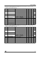
L78S00 SERIES ELECTRICAL CHARACTERISTICS OF L78S05C (refer to the test circuits, TJ = 25°C, VI = 10 V, IO = 500 mA, unless otherwise specified). Symbol Parameter Test Conditions VO Output Voltage VO Output Voltage IO = 1 A ∆VO Line Regulation VI = 7 to 25 V ∆VO Line Regulation VI = 7 V Min. ∆Id ∆VO/∆T Output Voltage Drift eN Unit 4.8 5 5.2 V 5 5.25 V 100 mV VI = 8 to 25 V 50 IO = 20 mA to 1.5 A 100 mV 8 mA mA 80 Quiescent Current Quiescent Current Change Max. 4.
L78S00 SERIES ELECTRICAL CHARACTERISTICS OF L78S09C (refer to the test circuits, TJ = 25°C, VI = 14 V, IO = 500 mA, unless otherwise specified). Symbol Parameter VO Output Voltage VO Output Voltage ∆VO Line Regulation ∆VO Line Regulation Test Conditions Typ. Max. 8.65 9 9.35 V 8.6 9 9.4 V VI = 11 to 25 V 130 mV VI = 11 to 20 V 65 IO = 1 A VI = 11 V Min. IO = 20 mA to 1.
L78S00 SERIES ELECTRICAL CHARACTERISTICS OF L78S12C (refer to the test circuits, TJ = 25°C, VI = 19 V, IO = 500 mA, unless otherwise specified). Symbol Parameter Test Conditions VO Output Voltage VO Output Voltage IO = 1 A ∆VO Line Regulation VI = 14.5 to 30 V ∆VO Line Regulation VI = 14.5 V Min. ∆Id ∆VO/∆T Output Voltage Drift eN Unit 11.5 12 12.5 V 12 12.6 V 240 mV VI = 16 to 22 V 120 IO = 20 mA to 1.5 A 240 mV 8 mA 0.
L78S00 SERIES ELECTRICAL CHARACTERISTICS OF L78S18C (refer to the test circuits, TJ = 25°C, VI = 26 V, IO = 500 mA, unless otherwise specified). Symbol Parameter VO Output Voltage VO Output Voltage ∆VO Line Regulation ∆VO Line Regulation Test Conditions Typ. Max. 17.1 18 18.9 V 17 18 19 V VI = 20.5 to 30 V 360 mV VI = 22 to 28 V 180 IO = 1 A VI = 20.5 V Min. IO = 20 mA to 1.5 A IO = 2 A Id ∆Id ∆VO/∆T Output Voltage Drift eN 360 mV 8 mA 0.
L78S00 SERIES Figure 4 : Dropout Voltage vs Junction Temperature Figure 7 : Output Voltage vs Junction Temperature Figure 5 : Peak Output Current vs Input/Output Differential Voltage Figure 8 : Output Impedance vs Frequency Figure 6 : Supply Voltage Rejection vs Frequency Figure 9 : Quiescent Current vs Junction Temperature 13/24
L78S00 SERIES Figure 10 : Load Transient Response Figure 11 : Line Transient Response 14/24 Figure 12 : Quiescent Current vs Input Voltage
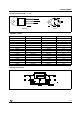
L78S00 SERIES Figure 13 : Fixed Output Regulator NOTE: 1. To specify an output voltage, substitute voltage value for "XX". 2. Although no output capacitor is need for stability, it does improve transient response. 3. Required if regulator is locate an appreciable distance from power supply filter.
L78S00 SERIES Figure 16 : Adjustable Output Regulator (7 to 30V) Figure 17 : 0.
L78S00 SERIES Figure 19 : High Output Current with Short Circuit Protection VBEQ2 RSC = ISC Figure 20 : Tracking Voltage Regulator Figure 21 : Positive and Negative Regulator * D1 and D2 are necessary if the load is connected between + VO and - VO.
L78S00 SERIES Figure 22 : Negative Output Voltage Circuit Figure 23 : Switching Regulator Figure 24 : High Input Voltage Circuit VIN = VI - (VZ + V BE) Figure 25 : High Input Voltage Circuit VIN = VZ - VBE 18/24
L78S00 SERIES Figure 26 : High Output Voltage Regulator Figure 27 : High Input and Output Voltage VO = VXX + VZ1 Figure 28 : Reducing Power Dissipation with Dropping Resistor VI(min) - VXX - VDROP(max) R = IO(max) + Id(max) Figure 29 : Remote Shutdown 19/24
L78S00 SERIES Figure 30 : Power AM Modulator (unity voltage gain, IO ≤ 1A) NOTE: The circuit performs well up to 100 KHz. Figure 31 : Adjustable Output Voltage with Temperature Compensation R2 VO = VXX (1+ ) + V BE R1 NOTE: Q2 is connected as a diode in order to compensate the variation of the Q1 VBE with the temperature. C allows a slow rise time of the VO.
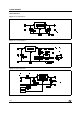
L78S00 SERIES Figure 33 : Protection against Input Short-Circuit with High Capacitance Loads Application with high capacitance loads and an output voltage greater than 6 volts need an external diode (see fig. 33) to protect the device against input short circuit. In this case the input voltage falls rapidly while the output voltage decrease slowly. The capacitance discharges by means of the Base-Emitter junction of the series pass transistor in the regulator.
L78S00 SERIES TO-220 MECHANICAL DATA DIM. mm. MIN. TYP inch MAX. MIN. TYP. MAX. A 4.40 4.60 0.173 0.181 C 1.23 1.32 0.048 0.051 D 2.40 2.72 0.094 0.107 D1 1.27 0.050 E 0.49 0.70 0.019 0.027 F 0.61 0.88 0.024 0.034 F1 1.14 1.70 0.044 0.067 F2 1.14 1.70 0.044 0.067 G 4.95 5.15 0.194 0.203 G1 2.4 2.7 0.094 0.106 H2 10.0 10.40 0.393 0.409 L2 16.4 0.645 L4 13.0 14.0 0.511 0.551 L5 2.65 2.95 0.104 0.116 L6 15.25 15.75 0.600 0.
L78S00 SERIES TO-3 MECHANICAL DATA mm. DIM. MIN. A inch TYP MAX. MIN. TYP. 11.85 B 0.96 MAX. 0.466 1.05 1.10 0.037 0.041 0.043 C 1.70 0.066 D 8.7 0.342 E 20.0 0.787 G 10.9 0.429 N 16.9 0.665 P 26.2 R 3.88 1.031 4.09 U 0.152 39.5 V 1.555 30.10 1.185 A P D C O N B V E G U 0.
L78S00 SERIES Information furnished is believed to be accurate and reliable. However, STMicroelectronics assumes no responsibility for the consequences of use of such information nor for any infringement of patents or other rights of third parties which may result from its use. No license is granted by implication or otherwise under any patent or patent rights of STMicroelectronics. Specifications mentioned in this publication are subject to change without notice.