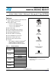
M24C16, M24C08 M24C04, M24C02, M24C01 16 Kbit, 8 Kbit, 4 Kbit, 2 Kbit and 1 Kbit serial I²C bus EEPROM Features ■ Supports both the 100 kHz I2C Standard-mode and the 400 kHz I2C Fast-mode ■ Single supply voltage: – 2.5 V to 5.5 V for M24Cxx-W – 1.8 V to 5.5 V for M24Cxx-Rev 16 – 1.7 V to 5.
Contents M24C16, M24C08, M24C04, M24C02, M24C01 Contents 1 Description . . . . . . . . . . . . . . . . . . . . . . . . . . . . . . . . . . . . . . . . . . . . . . . . . 6 2 Signal description . . . . . . . . . . . . . . . . . . . . . . . . . . . . . . . . . . . . . . . . . . . 8 2.1 Serial Clock (SCL) . . . . . . . . . . . . . . . . . . . . . . . . . . . . . . . . . . . . . . . . . . . 8 2.2 Serial Data (SDA) . . . . . . . . . . . . . . . . . . . . . . . . . . . . . . . . . . . . . . . . . . . .
M24C16, M24C08, M24C04, M24C02, M24C01 Contents 7 Package mechanical data . . . . . . . . . . . . . . . . . . . . . . . . . . . . . . . . . . . . 26 8 Part numbering . . . . . . . . . . . . . . . . . . . . . . . . . . . . . . . . . . . . . . . . . . . . 32 9 Revision history . . . . . . . . . . . . . . . . . . . . . . . . . . . . . . . . . . . . . . . . . . .
List of tables M24C16, M24C08, M24C04, M24C02, M24C01 List of tables Table 1. Table 2. Table 3. Table 4. Table 5. Table 6. Table 7. Table 8. Table 9. Table 10. Table 11. Table 12. Table 13. Table 14. Table 15. Table 16. Table 17. Table 18. Table 19. Table 20. Table 21. Table 22. Table 23. Table 24. Table 25. Table 26. Table 27. Table 28. Table 29. Table 30. 4/39 Device summary . . . . . . . . . . . . . . . . . . . . . . . . . . . . . . . . . . . . . . . . . . . . . . . . . . . . . . . . . .
M24C16, M24C08, M24C04, M24C02, M24C01 List of figures List of figures Figure 1. Figure 2. Figure 3. Figure 4. Figure 5. Figure 6. Figure 7. Figure 8. Figure 9. Figure 10. Figure 11. Figure 12. Figure 13. Figure 14. Figure 15. Figure 16. Figure 17. Logic diagram . . . . . . . . . . . . . . . . . . . . . . . . . . . . . . . . . . . . . . . . . . . . . . . . . . . . . . . . . . . . 6 8-pin package connections (top view) . . . . . . . . . . . . . . . . . . . . . . . . . . . . . . . . . . . . . . . . .
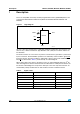
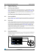
Description 1 M24C16, M24C08, M24C04, M24C02, M24C01 Description These I²C-compatible electrically erasable programmable memory (EEPROM) devices are organized as 2048/1024/512/256/128 x 8 (M24C16, M24C08, M24C04, M24C02 and M24C01). Figure 1. Logic diagram VCC 3 E0-E2 SDA M24Cxx SCL WC VSS AI02033 I²C uses a two-wire serial interface, comprising a bidirectional data line and a clock line.
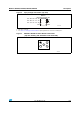
M24C16, M24C08, M24C04, M24C02, M24C01 Figure 2. Description 8-pin package connections (top view) M24Cxx 16Kb /8Kb /4Kb /2Kb /1Kb NC / NC / NC / E0 / E0 1 8 VCC NC / NC / E1 / E1 / E1 2 7 WC NC / E2 / E2 / E2 / E2 3 6 SCL VSS 4 5 SDA AI02034E 1. NC = Not connected 2. See Section 7: Package mechanical data for package dimensions, and how to identify pin-1. Figure 3.
Signal description M24C16, M24C08, M24C04, M24C02, M24C01 2 Signal description 2.1 Serial Clock (SCL) This input signal is used to strobe all data in and out of the device. In applications where this signal is used by slave devices to synchronize the bus to a slower clock, the bus master must have an open drain output, and a pull-up resistor can be connected from Serial Clock (SCL) to VCC. (Figure 5 indicates how the value of the pull-up resistor can be calculated).
M24C16, M24C08, M24C04, M24C02, M24C01 2.4 Supply voltage (VCC) 2.4.1 Operating supply voltage VCC Signal description Prior to selecting the memory and issuing instructions to it, a valid and stable VCC voltage within the specified [VCC(min), VCC(max)] range must be applied (see Table 6, Table 7 and Table 8). In order to secure a stable DC supply voltage, it is recommended to decouple the VCC line with a suitable capacitor (usually of the order of 10 nF to 100 nF) close to the VCC/VSS package pins.
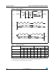
Signal description Figure 6. M24C16, M24C08, M24C04, M24C02, M24C01 I²C bus protocol SCL SDA SDA Input Start condition SCL 1 2 SDA MSB SDA Change Stop condition 3 7 8 9 ACK Start condition SCL 1 SDA MSB 2 3 7 8 9 ACK Stop condition AI00792c Table 3.
M24C16, M24C08, M24C04, M24C02, M24C01 3 Device operation Device operation The device supports the I²C protocol. This is summarized in Figure 6. Any device that sends data on to the bus is defined to be a transmitter, and any device that reads the data to be a receiver. The device that controls the data transfer is known as the bus master, and the other as the slave device. A data transfer can only be initiated by the bus master, which will also provide the serial clock for synchronization.
Device operation 3.5 M24C16, M24C08, M24C04, M24C02, M24C01 Memory addressing To start communication between the bus master and the slave device, the bus master must initiate a Start condition. Following this, the bus master sends the device select code, shown in Table 3 (on Serial Data (SDA), most significant bit first). The device select code consists of a 4-bit Device Type Identifier, and a 3-bit Chip Enable “Address” (E2, E1, E0).
M24C16, M24C08, M24C04, M24C02, M24C01 Figure 7. Device operation Write mode sequences with WC = 1 (data write inhibited) WC ACK Byte address NO ACK Data in Stop Dev select Start Byte Write ACK R/W WC ACK Dev select Start Page Write ACK Byte address NO ACK Data in 1 NO ACK Data in 2 Data in 3 R/W WC (cont'd) NO ACK Data in N Stop Page Write (cont'd) NO ACK AI02803d 3.
Device operation M24C16, M24C08, M24C04, M24C02, M24C01 the addressed location is not Write-protected, the device replies with Ack. The bus master terminates the transfer by generating a Stop condition, as shown in Figure 8. 3.6.2 Page Write The Page Write mode allows up to 16 bytes to be written in a single Write cycle, provided that they are all located in the same page in the memory: that is, the most significant memory address bits are the same.
M24C16, M24C08, M24C04, M24C02, M24C01 Figure 9.
Device operation M24C16, M24C08, M24C04, M24C02, M24C01 Figure 10.
M24C16, M24C08, M24C04, M24C02, M24C01 3.7.2 Device operation Current Address Read For the Current Address Read operation, following a Start condition, the bus master only sends a device select code with the Read/Write bit (RW) set to 1. The device acknowledges this, and outputs the byte addressed by the internal address counter. The counter is then incremented. The bus master terminates the transfer with a Stop condition, as shown in Figure 10, without acknowledging the byte. 3.7.
Initial delivery state 4 M24C16, M24C08, M24C04, M24C02, M24C01 Initial delivery state The device is delivered with all bits in the memory array set to 1 (each byte contains FFh). 5 Maximum rating Stressing the device outside the ratings listed in Table 5 may cause permanent damage to the device. These are stress ratings only, and operation of the device at these, or any other conditions outside those indicated in the operating sections of this specification, is not implied.
M24C16, M24C08, M24C04, M24C02, M24C01 6 DC and AC parameters DC and AC parameters This section summarizes the operating and measurement conditions, and the DC and AC characteristics of the device. The parameters in the DC and AC characteristic tables that follow are derived from tests performed under the measurement conditions summarized in the relevant tables. Designers should check that the operating conditions in their circuit match the measurement conditions when relying on the quoted parameters.
DC and AC parameters Table 9. M24C16, M24C08, M24C04, M24C02, M24C01 DC characteristics (M24Cxx-W, device grade 6) Symbol Test conditions (in addition to those in Table 6) Parameter ILI Input leakage current V = VSS or VCC, device in Standby mode (SCL, SDA, E0, E1,and E2) IN ILO Output leakage current ICC Min. Max. Unit ±2 µA SDA in Hi-Z, external voltage applied on SDA: VSS or VCC ±2 µA VCC = 5 V, fc = 400 kHz (rise/fall time < 50 ns) 2 mA VCC = 2.
M24C16, M24C08, M24C04, M24C02, M24C01 Table 11. DC and AC parameters DC characteristics (M24Cxx-R) Symbol Parameter Test condition (in addition to those in Table 7) ILI Input leakage current (SCL, SDA, E0, E1,and E2) ILO Output leakage current ICC Supply current ICC1 Standby supply current VIL Input low voltage (SDA, SCL, WC) VIH Input high voltage (SDA, SCL, WC) VOL Output low voltage Min. Max.
DC and AC parameters Table 12. M24C16, M24C08, M24C04, M24C02, M24C01 DC characteristics (M24Cxx-F) Symbol Test condition (in addition to those in Table 8) Parameter ILI Input leakage current (SCL, SDA, E0, E1,and E2) ILO Output leakage current ICC Supply current ICC1 Standby supply current VIL Input low voltage (SDA, SCL, WC) VIH Input high voltage (SDA, SCL, WC) VOL Output low voltage Min. Max.
M24C16, M24C08, M24C04, M24C02, M24C01 Table 15. DC and AC parameters AC characteristics at 400 kHz (I2C Fast-mode) (M24Cxx-W, M24Cxx-R, M24Cxx-F) Test conditions specified in either Table 6, Table 7 or Table 8 and Table 13 Max.(1) Unit 400 kHz Alt. fC fSCL Clock frequency tCHCL tHIGH Clock pulse width high 600 ns tCLCH tLOW Clock pulse width low 1300 ns tQL1QL2 (2) tXH1XH2 tXL1XL2 tF tR tF Parameter Min.
DC and AC parameters Table 16. M24C16, M24C08, M24C04, M24C02, M24C01 AC characteristics at 100 kHz (I2C Standard-mode)(1) (M24Cxx-W, M24Cxx-R, M24Cxx-F) Test conditions specified in either Table 6, Table 7 or Table 8 and Table 13 Symbol Alt. fC fSCL tCHCL Min. Max. Unit Clock frequency - 100 kHz tHIGH Clock pulse width high 4 - µs tCLCH tLOW Clock pulse width low 4.
M24C16, M24C08, M24C04, M24C02, M24C01 DC and AC parameters Figure 12.
Package mechanical data 7 M24C16, M24C08, M24C04, M24C02, M24C01 Package mechanical data In order to meet environmental requirements, ST offers these devices in different grades of ECOPACK® packages, depending on their level of environmental compliance. ECOPACK® specifications, grade definitions and product status are available at: www.st.com. ECOPACK® is an ST trademark. Figure 13. WLCSP (0.5 mm) and Thin WLCSP (0.3 mm) 0.
M24C16, M24C08, M24C04, M24C02, M24C01 Table 18. Package mechanical data M24C08: Thin WLCSP (0.3 mm height), 0.4 mm pitch, 5 bumps, package data(1) inches(2) millimeters Symbol Typ Min Max Typ Min Max A 0.3 0.270 0.330 0.0118 0.0096 0.014 A1 0.1 0.0039 A2 0.2 0.0079 b 0.16 0.0063 D 1.215 1.34 0.0478 0.0528 E 1.025 1.15 0.0404 0.0453 e 0.4 0.0157 e1 0.693 0.0273 e2 0.346 0.0136 F 0.313 0.0123 G 0.261 0.0103 N(3) 5 5 1. Preliminary data. 2.
Package mechanical data M24C16, M24C08, M24C04, M24C02, M24C01 Figure 14. SO8 narrow – 8 lead plastic small outline, 150 mils body width, package outline h x 45˚ A2 A c ccc b e 0.25 mm GAUGE PLANE D k 8 E1 E 1 L A1 L1 SO-A 1. Drawing is not to scale. 2. The ‘1’ that appears in the top view of the package shows the position of pin 1 and the ‘N’ indicates the total number of pins. Table 20.
M24C16, M24C08, M24C04, M24C02, M24C01 Package mechanical data Figure 15. UFDFPN8 (MLP8) 8-lead ultra thin fine pitch dual flat package no lead 2 x 3 mm, outline REV MB e D REV MC e b L1 L3 b L1 L3 Pin 1 E E2 E2 K K L L A D2 D2 ddd A1 ZW_MEc 1. Drawing is not to scale. 2. The central pad (the area E2 by D2 in the above illustration) is pulled, internally, to VSS. It must not be allowed to be connected to any other voltage or signal line on the PCB, for example during the soldering process.
Package mechanical data M24C16, M24C08, M24C04, M24C02, M24C01 Figure 16. TSSOP8 – 8 lead thin shrink small outline, package outline D 8 5 c E1 1 E 4 α A1 A L A2 L1 CP b e TSSOP8AM 1. Drawing is not to scale. 2. The circle in the top view of the package indicates the position of pin 1. Table 22. TSSOP8 – 8 lead thin shrink small outline, package mechanical data inches(1) millimeters Symbol Typ. Min. A Max. 0.050 0.150 0.800 1.050 b 0.190 c 0.090 1.000 CP Max. 0.0472 0.
M24C16, M24C08, M24C04, M24C02, M24C01 Package mechanical data Figure 17. PDIP8 – 8 pin plastic DIP, 0.25 mm lead frame, package outline E b2 A2 A1 b A L c e eA eB D 8 E1 1 PDIP-B 1. Drawing is not to scale. Table 23. PDIP8 – 8 pin plastic DIP, 0.25 mm lead frame, package mechanical data inches(1) millimeters Symbol Typ. Min. A Max. Typ. Min. 5.33 A1 Max. 0.2098 0.38 0.015 A2 3.3 2.92 4.95 0.1299 0.115 0.1949 b 0.46 0.36 0.56 0.0181 0.0142 0.022 b2 1.52 1.14 1.78 0.
Part numbering 8 M24C16, M24C08, M24C04, M24C02, M24C01 Part numbering Table 24. Ordering information scheme Example: M24C16 – W DW 3 T P /S Device type M24 = I2C serial access EEPROM Device Function 16 = 16 Kbit (2048 x 8) 08 = 8 Kbit (1024 x 8) 04 = 4 Kbit (512 x 8) 02 = 2 Kbit (256 x 8) 01 = 1 Kbit (128 x 8) Operating voltage W = VCC = 2.5 V to 5.5 V (400 kHz) R = VCC = 1.8 V to 5.5 V (400 kHz) F = VCC = 1.7 V to 5.
M24C16, M24C08, M24C04, M24C02, M24C01 Table 25. Part numbering Available M24C16 products (package, voltage range, temperature grade) M24C16-W VCC = 2.5 V to 5.5 V M24C16-R VCC = 1.8 V to 5.5 V M24C16-F VCC = 1.7 V to 5.5 V Range 6 Range 6 - Range 6, Range 3 Range 6 - UFDFPN8 (MB) - Range 6 Range 5 UFDFPN8 (MC) - Range 6 - TSSOP8 (DW) Range 6, Range 3 Range 6 - - - Range 5 Package DIP8 (BN) SO8N (MN) WLCSP (CS) Table 26.
Part numbering M24C16, M24C08, M24C04, M24C02, M24C01 Table 28. Available M24C02 products (package, voltage range, temperature grade) Package DIP8 (BN) SO8N (MN) UFDFPN8 (MB or MC) TSSOP8 (DW) Table 29. M24C02-R VCC = 1.8 V to 5.5 V Range 6 - Range 6, Range 3 Range 6 - Range 6 Range 6, Range 3 Range 6 Available M24C01 products (package, voltage range, temperature grade) M24C01-W VCC = 2.5 V to 5.5 V M24C01-R VCC = 1.8 V to 5.
M24C16, M24C08, M24C04, M24C02, M24C01 9 Revision history Revision history Table 30. Document revision history Date Version 10-Dec-1999 2.4 TSSOP8 Turned-Die package removed (p 2 and order information) Lead temperature added for TSSOP8 in table 2 18-Apr-2000 2.5 Labelling change to Fig-2D, correction of values for ‘E’ and main caption for Tab-13 05-May-2000 2.6 Extra labelling to Fig-2D 23-Nov-2000 3.
Revision history Table 30. Date 7-Oct-2005 17-Jan-2006 19-Sep-2006 03-Aug-2007 27-Sep-2007 36/39 M24C16, M24C08, M24C04, M24C02, M24C01 Document revision history (continued) Version Changes 6.0 Product List summary table added. AEC-Q100-002 compliance. Device Grade information clarified. Updated Device internal reset section, Figure 4, Figure 5, Table 16 and Table 24 Added ECOPACK® information. Updated tW=5ms for the M24Cxx-W. 7.0 Pin numbers removed from silhouettes (see on page 1).
M24C16, M24C08, M24C04, M24C02, M24C01 Table 30. Date Revision history Document revision history (continued) Version Changes 30-Jan-2009 11 Section 2.4: Supply voltage (VCC) clarified. Figure 5: Maximum RP value versus bus parasitic capacitance (C) for an I²C bus updated. IOL added to Table 5: Absolute maximum ratings. ICC1 test conditions clarified in DC characteristics Table 9, Table 10, Table 11 and Table 12. Note modified below Table 14: Input parameters.
Revision history Table 30. Date 01-Apr-2010 29-Apr-2010 38/39 M24C16, M24C08, M24C04, M24C02, M24C01 Document revision history (continued) Version Changes 15 Updated Figure 15: UFDFPN8 (MLP8) 8-lead ultra thin fine pitch dual flat package no lead 2 x 3 mm, outline and Table 21 on page 29. Updated Table 13: AC measurement conditions. Updated Table 25 to Table 27. 16 Deleted TSSOP8 3x3 mm package from cover page. Deleted Figure and Table relating to TSSOP8 3x3 mm package information.
M24C16, M24C08, M24C04, M24C02, M24C01 Please Read Carefully: Information in this document is provided solely in connection with ST products. STMicroelectronics NV and its subsidiaries (“ST”) reserve the right to make changes, corrections, modifications or improvements, to this document, and the products and services described herein at any time, without notice. All ST products are sold pursuant to ST’s terms and conditions of sale.