
Datasheet

Description M24C16, M24C08, M24C04, M24C02, M24C01
6/39 Doc ID 5067 Rev 16
1 Description
These I²C-compatible electrically erasable programmable memory (EEPROM) devices are
organized as 2048/1024/512/256/128
x 8 (M24C16, M24C08, M24C04, M24C02 and
M24C01).
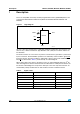
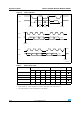
Figure 1. Logic diagram
I²C uses a two-wire serial interface, comprising a bidirectional data line and a clock line. The
devices carry a built-in 4-bit Device Type Identifier code (1010) in accordance with the I²C
bus definition.
The device behaves as a slave in the I²C protocol, with all memory operations synchronized
by the serial clock. Read and Write operations are initiated by a Start condition, generated
by the bus master. The Start condition is followed by a device select code and Read/
Write
bit (R
W) (as described in Ta b l e 3), terminated by an acknowledge bit.
When writing data to the memory, the device inserts an acknowledge bit during the 9
th
bit
time, following the bus master’s 8-bit transmission. When data is read by the bus master, the
bus master acknowledges the receipt of the data byte in the same way. Data transfers are
terminated by a Stop condition after an Ack for Write, and after a NoAck for Read.
Table 2. Signal names
Signal name Function Direction
E0, E1, E2 Chip Enable Input
SDA Serial Data Input/output
SCL Serial Clock Input
WC
Write Control Input
V
CC
Supply voltage
V
SS
Ground
AI02033
3
E0-E2 SDA
V
CC
M24Cxx
WC
SCL
V
SS