
Datasheet
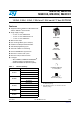

Signal description M24C16, M24C08, M24C04, M24C02, M24C01
8/39 Doc ID 5067 Rev 16
2 Signal description
2.1 Serial Clock (SCL)
This input signal is used to strobe all data in and out of the device. In applications where this
signal is used by slave devices to synchronize the bus to a slower clock, the bus master
must have an open drain output, and a pull-up resistor can be connected from Serial Clock
(SCL) to V
CC
. (Figure 5 indicates how the value of the pull-up resistor can be calculated). In
most applications, though, this method of synchronization is not employed, and so the pull-
up resistor is not necessary, provided that the bus master has a push-pull (rather than open
drain) output.
2.2 Serial Data (SDA)
This bidirectional signal is used to transfer data in or out of the device. It is an open drain
output that may be wire-ORed with other open drain or open collector signals on the bus. A
pull up resistor must be connected from Serial Data (SDA) to V
CC
. (Figure 5 indicates how
the value of the pull-up resistor can be calculated).
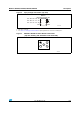
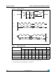
2.3 Chip Enable (E0, E1, E2)
These input signals are used to set the value that is to be looked for on the three least
significant bits (b3, b2, b1) of the 7-bit device select code. These inputs must be tied to V
CC
or V
SS
, to establish the device select code as shown in Figure 4. When not connected (left
floating), E0, E1, E2 are read as low (0,0,0).
Figure 4. Device select code
2.3.1 Write Control (WC)
This input signal is useful for protecting the entire contents of the memory from inadvertent
write operations. Write operations are disabled to the entire memory array when Write
Control (
WC) is driven High. When unconnected, the signal is internally read as V
IL
, and
Write operations are allowed.
When Write Control (WC) is driven High, device select and address bytes are
acknowledged, data bytes are not acknowledged.
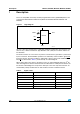
Ai11650
V
CC
M24Cxx
V
SS
E
i
V
CC
M24Cxx
V
SS
E
i