M48T35 M48T35Y 5 V, 256 Kbit (32 Kb x 8) TIMEKEEPER® SRAM Features ■ Integrated, ultra low power SRAM, real-time clock, power-fail control circuit and battery ■ BYTEWIDE™ RAM-like clock access ■ BCD coded year, month, day, date, hours, minutes, and seconds ■ Frequency test output for real-time clock ■ Automatic power-fail chip deselect and WRITE protection ■ WRITE protect voltages VPFD = power-fail deselect voltage): – M48T35: VCC = 4.75 to 5.5 V; 4.5 V ≤ VPFD ≤ 4.75 V – M48T35Y: VCC = 4.5 to 5.
Contents M48T35, M48T35Y Contents 1 Description . . . . . . . . . . . . . . . . . . . . . . . . . . . . . . . . . . . . . . . . . . . . . . . . . 5 2 Operation modes . . . . . . . . . . . . . . . . . . . . . . . . . . . . . . . . . . . . . . . . . . . . 8 3 2.1 READ mode . . . . . . . . . . . . . . . . . . . . . . . . . . . . . . . . . . . . . . . . . . . . . . . . 8 2.2 WRITE mode . . . . . . . . . . . . . . . . . . . . . . . . . . . . . . . . . . . . . . . . . . . . . . 10 2.
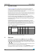
M48T35, M48T35Y List of tables List of tables Table 1. Table 2. Table 3. Table 4. Table 5. Table 6. Table 7. Table 8. Table 9. Table 10. Table 11. Table 12. Table 13. Table 14. Table 15. Table 16. Table 17. Table 18. Signal names . . . . . . . . . . . . . . . . . . . . . . . . . . . . . . . . . . . . . . . . . . . . . . . . . . . . . . . . . . . . 6 Operating modes . . . . . . . . . . . . . . . . . . . . . . . . . . . . . . . . . . . . . . . . . . . . . . . . . . . . . . . . .
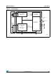
List of figures M48T35, M48T35Y List of figures Figure 1. Figure 2. Figure 3. Figure 4. Figure 5. Figure 6. Figure 7. Figure 8. Figure 9. Figure 10. Figure 11. Figure 12. Figure 13. Figure 14. Figure 15. Figure 16. Figure 17. 4/28 Logic diagram . . . . . . . . . . . . . . . . . . . . . . . . . . . . . . . . . . . . . . . . . . . . . . . . . . . . . . . . . . . . 5 DIP connections . . . . . . . . . . . . . . . . . . . . . . . . . . . . . . . . . . . . . . . . . . . . . . . . . . . . . . . . . .
M48T35, M48T35Y 1 Description Description The M48T35/Y TIMEKEEPER® RAM is a 32 Kb x 8 non-volatile static RAM and real-time clock. The monolithic chip is available in two special packages to provide a highly integrated battery-backed memory and real-time clock solution. The M48T35/Y is a non-volatile pin and function equivalent to any JEDEC standard 32 Kb x 8 SRAM.
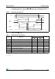
Description M48T35, M48T35Y Table 1. Signal names A0-A14 Address inputs DQ0-DQ7 Data inputs / outputs E Chip enable G Output enable W WRITE enable VCC Supply voltage VSS Ground Figure 2. DIP connections A14 A12 A7 A6 A5 A4 A3 A2 A1 A0 DQ0 DQ1 DQ2 VSS Figure 3.
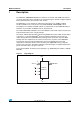
M48T35, M48T35Y Figure 4.
Operation modes 2 M48T35, M48T35Y Operation modes As Figure 4 on page 7 shows, the static memory array and the quartz controlled clock oscillator of the M48T35/Y are integrated on one silicon chip. The two circuits are interconnected at the upper eight memory locations to provide user accessible BYTEWIDE clock information in the bytes with addresses 7FF8h-7FFFh. The clock locations contain the year, month, date, day, hour, minute, and second in 24-hour BCD format.
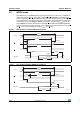
M48T35, M48T35Y Operation modes If the address inputs are changed while E and G remain active, output data will remain valid for output data hold time (tAXQX) but will go indeterminate until the next address access. Figure 5. READ mode AC waveforms tAVAV VALID A0-A14 tAVQV tAXQX tELQV tEHQZ E tELQX tGLQV tGHQZ G tGLQX DQ0-DQ7 VALID AI00925 Note: WRITE enable (W) = high. Table 3.
Operation modes 2.2 M48T35, M48T35Y WRITE mode The M48T35/Y is in the WRITE mode whenever W and E are low. The start of a WRITE is referenced from the latter occurring falling edge of W or E. A WRITE is terminated by the earlier rising edge of W or E. The addresses must be held valid throughout the cycle. E or W must return high for a minimum of tEHAX from chip enable or tWHAX from WRITE enable prior to the initiation of another READ or WRITE cycle.
M48T35, M48T35Y Table 4.
Clock operations 3 Clock operations 3.1 Reading the clock M48T35, M48T35Y Updates to the TIMEKEEPER® registers (see Table 5) should be halted before clock data is read to prevent reading data in transition. The BiPORT™ TIMEKEEPER cells in the RAM array are only data registers and not the actual clock counters, so updating the registers can be halted without disturbing the clock itself. Updating is halted when a '1' is written to the READ bit, D6 in the control register 7FF8h.
M48T35, M48T35Y Table 5. Clock operations Register map Data Function/range Address D7 D6 7FFEh 0 0 7FFDh 0 0 7FFCh 0 FT 7FFBh 0 0 7FFAh 0 7FF9h ST 7FF8h W 7FFFh D5 D4 D3 D2 10 Years 0 Year 00-99 Month 01-12 Date Date 01-31 Century/ day 00-01/01-07 Hours Hours 00-23 Minutes Minutes 00-59 Seconds Seconds 00-59 0 Day 10 hours 10 minutes 10 seconds R S BCD format Year 10 date CB D0 Month 10 M.
Clock operations M48T35, M48T35Y sign bit; '1' indicates positive calibration, '0' indicates negative calibration. Calibration occurs within a 64 minute cycle. The first 62 minutes in the cycle may, once per minute, have one second either shortened by 128 or lengthened by 256 oscillator cycles. If a binary '1' is loaded into the register, only the first 2 minutes in the 64 minute cycle will be modified; if a binary 6 is loaded, the first 12 will be affected, and so on.
M48T35, M48T35Y Clock operations Figure 8. Crystal accuracy across temperature ppm 20 0 -20 -40 ΔF = -0.038 ppm (T - T )2 ± 10% 0 F C2 -60 T0 = 25 °C -80 -100 0 5 10 15 20 25 30 35 40 45 50 55 60 65 70 °C AI02124 Figure 9.
Clock operations 3.6 M48T35, M48T35Y VCC noise and negative going transients ICC transients, including those produced by output switching, can produce voltage fluctuations, resulting in spikes on the VCC bus. These transients can be reduced if capacitors are used to store energy which stabilizes the VCC bus. The energy stored in the bypass capacitors will be released as low going spikes are generated or energy will be absorbed when overshoots occur. A bypass capacitor value of 0.
M48T35, M48T35Y 4 Maximum ratings Maximum ratings Stressing the device above the rating listed in the absolute maximum ratings table may cause permanent damage to the device. These are stress ratings only and operation of the device at these or any other conditions above those indicated in the operating sections of this specification is not implied. Exposure to absolute maximum rating conditions for extended periods may affect device reliability. Table 6.
DC and AC parameters 5 M48T35, M48T35Y DC and AC parameters This section summarizes the operating and measurement conditions, as well as the DC and AC characteristics of the device. The parameters in the following DC and AC characteristic tables are derived from tests performed under the measurement conditions listed in the relevant tables. Designers should check that the operating conditions in their projects match the measurement conditions when using the quoted parameters. Table 7.
M48T35, M48T35Y DC and AC parameters Table 9. DC characteristics Symbol Parameter M48T35 Test condition(1) M48T35Y Unit Min Max Min Max ILI Input leakage current 0 V ≤ VIN ≤ VCC ±1 ±1 µA ILO(2) Output leakage current 0 V ≤ VOUT ≤ VCC ±1 ±1 µA ICC Supply current Outputs open 50 30 mA ICC1 Supply current (standby) TTL E = VIH 3 3 mA ICC2 Supply current (standby) CMOS E = VCC – 0.2 V 2 2 mA VIL Input low voltage –0.3 0.8 –0.3 0.8 V VIH Input high voltage 2.
DC and AC parameters Table 10. M48T35, M48T35Y Power down/up AC characteristics Parameter(1) Symbol tPD tF (2) tFB(3) Min E or W at VIH before power down VPFD (max) to VPFD (min) VCC fall time VPFD (min) to VSS VCC fall time Max Unit 0 µs 300 µs M48T35 10 µs M48T35Y 10 µs tR VPFD (min) to VPFD (max) VCC rise time 10 µs tRB VSS to VPFD (min) VCC rise time 1 µs trec(4) VPFD (max) to inputs recognized 40 200 ms 1.
M48T35, M48T35Y 6 Package mechanical data Package mechanical data In order to meet environmental requirements, ST offers these devices in different grades of ECOPACK® packages, depending on their level of environmental compliance. ECOPACK® specifications, grade definitions and product status are available at: www.st.com. ECOPACK® is an ST trademark. Figure 13. PCDIP28 – 28-pin plastic DIP, battery CAPHAT™, package outline A2 A1 B1 B A L C e1 eA e3 D N E 1 PCDIP Note: Drawing is not to scale.
Package mechanical data M48T35, M48T35Y Figure 14. SOH28 – 28-lead plastic small outline, 4-socket battery SNAPHAT®, package outline A2 A C B eB e CP D N E H A1 α L 1 Note: SOH-A Drawing is not to scale. Table 13. SOH28 – 28-lead plastic SO, 4-socket battery SNAPHAT®, package mechanical data mm inches Symbol Typ Min A Typ Min 3.05 Max 0.120 A1 0.05 0.36 0.002 0.014 A2 2.34 2.69 0.092 0.106 B 0.36 0.51 0.014 0.020 C 0.15 0.32 0.006 0.012 D 17.71 18.49 0.
M48T35, M48T35Y Package mechanical data Figure 15. SH – 4-pin SNAPHAT® housing for 48 mAh battery & crystal, package outline A1 A2 A3 A eA B L eB D E SHTK Note: Drawing is not to scale. Table 14. SH – 4-pin SNAPHAT® housing for 48 mAh battery & crystal, package mechanical data mm inches Symbol Typ Min A Max Typ Min 9.78 Max 0.385 A1 6.73 7.24 0.265 0.285 A2 6.48 6.99 0.255 0.275 B 0.46 0.56 0.018 0.022 D 21.21 21.84 0.835 0.860 E 14.22 14.99 0.560 0.
Package mechanical data M48T35, M48T35Y Figure 16. SH – 4-pin SNAPHAT® housing for 120 mAh battery & crystal, package outline A1 A2 A3 A eA B L eB D E SHTK Note: Drawing is not to scale. Table 15. SH – 4-pin SNAPHAT® housing for 120 mAh battery & crystal, package mechanical data mm inches Symbol Typ Min A Typ Min 10.54 Max 0.415 A1 8.00 8.51 0.315 0.335 A2 7.24 8.00 0.285 0.315 B 0.46 0.56 0.018 0.022 D 21.21 21.84 0.835 0.860 E 17.27 18.03 0.680 0.710 eB 3.
M48T35, M48T35Y 7 Part numbering Part numbering Table 16. Ordering information scheme Example: M48T 35 –70 PC 1 E Device type M48T Supply voltage and write protect voltage 35(1) = VCC = 4.75 to 5.5 V; VPFD = 4.5 to 4.75 V 35Y(2) = VCC = 4.5 to 5.5 V; VPFD = 4.2 to 4.
Environmental information 8 M48T35, M48T35Y Environmental information Figure 17. Recycling symbols This product contains a non-rechargeable lithium (lithium carbon monofluoride chemistry) button cell battery fully encapsulated in the final product. Recycle or dispose of batteries in accordance with the battery manufacturer's instructions and local/national disposal and recycling regulations.
M48T35, M48T35Y 9 Revision history Revision history Table 18. Document revision history Date Revision Nov-1999 1 07-Feb-2000 1.1 Changes First issue tDR description changed (Table 9) Reformatted; temp/voltage info. added to tables (Table 8, 9, 3, 4, 10, 11); add century bit text 04-Jun-2001 2 31-Jul-2001 2.1 Formatting changes based on latest document reviews 06-Mar-2002 2.2 Add PMDIP packaging option, which is “Not for New Design” (NND) (Table 16) 20-May-2002 2.
M48T35, M48T35Y Please Read Carefully: Information in this document is provided solely in connection with ST products. STMicroelectronics NV and its subsidiaries (“ST”) reserve the right to make changes, corrections, modifications or improvements, to this document, and the products and services described herein at any time, without notice. All ST products are sold pursuant to ST’s terms and conditions of sale.