
Datasheet


M54HC4094
M74HC4094
February 1993
8 BIT SIPO SHIFT LATCH REGISTER (3-STATE)
B1R
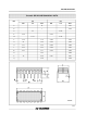
(Plastic Package)
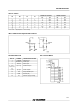
ORDER CODES :
M54HC4094F1R M74HC4094M1R
M74HC4094B1R M74HC4094C1R
F1R
(Ceramic Package)
M1R
(Micro Package)
C1R
(Chip Carrier)
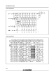
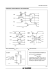
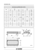
PIN CONNECTIONS (top view)
NC =
No Internal
Connection
DESCRIPTION
.HIGH SPEED
f
MAX
= 73 MHz (TYP.) AT V
CC
=5V
.LOW POWER DISSIPATION
I
CC
=4µA (MAX.) AT T
A
=25°C
.HIGH NOISE IMMUNITY
V
NIH
=V
NIL
=28%V
CC
(MIN.)
.OUTPUT DRIVE CAPABILITY
10 LSTTL LOADS
.SYMMETRICAL OUTPUT IMPEDANCE
|I
OH
|=I
OL
= 4 mA (MIN.)
.BALANCEDPROPAGATION DELAYS
t
PLH
=t
PHL
.WIDE OPERATING VOLTAGE RANGE
V
CC
(OPR) = 2 V TO 6 V
.PIN AND FUNCTION COMPATIBLE
WITH 4094B
The M54/74HC4094 is a high speed CMOS 8 BIT
SIPOSHIFTLATCH REGISTERfabricated withsili-
con gate C
2
MOS technology.
It has the same high speed performance of LSTTL
combined with true CMOS low power consumption.
This device consists of an 8-bit shift register and an
8-bit latch with 3-state output buffer. Data is shifted
serially through the shift register on the positive
going transition of the clock input signal. The output
of the last stage (Qs) can be used to cascade sev-
eral devices.
Dataon the Qsoutput is transferred toa second out-
put (Qs’) on the following negative transition of the
clockinput signal. The data of eachstage of the shift
register is provided with a latch, which latches data
on the negative going transition of the STROBE
input signal. When the STROBE input is held high,
datapropagates through thelatchto a3-state output
buffer.
This buffer is enabled when OUTPUT ENABLE
input is taken high. All inputs are equipped with pro-
tectioncircuits against static discharge and transient
excess voltage.
1/12