
Datasheet


ST662AB, ST662AC Description
Doc ID 5068 Rev 8 9/20
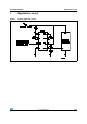
6 Description
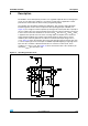
The ST662 is an IC developed to provide a 12 V regulated output 30 mA from voltage input
as low as 4.75 without any inductors. It is useful for a wide range of applications and its
performances make it ideal for Flash memory programming supply.
An evaluation kit is provided to facilitate the application. This include a single-side demo
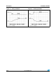
board designed for surface-mount components.The operating principle of ST662 (see
Figure 12) is to charge C1 and C2 capacitor by closing the S1 switch (while S2 is opened) at
the V
CC
voltage. After S1 is opened and S2 closed so that C1 and C2 capacitors are placed
in series one to each other, and both are in series with V
IN
. The sum of V
C1
and V
C2
and V
I
is applied to the capacitor C4. This works as voltage triple. An amplifier error checks the
output voltage and blocks the oscillator if the output voltage is greater than 12 V. The
shutdown pin is internally pulled to V
CC
. When it is held low the output voltage rises to
+12 V. Figure 13 shows the transition time of the shut down pin when the V
SHDN
goes from
5 V to 0 V. Input logic levels of this input are CMOS compatible Applying a logic high at this
input, the V
OUT
oscillator is blocked and the V
OUT
is reach the V
I
value by D1. In this
condition I
CC
is low as 1 µA. The Figure 14 shows the transition time of the shut down pin
when the V
SHDN
goes from 0 V to 5 V.
Figure 12. Operating principle circuit