
Datasheet

STP5NK80Z - STP5NK80ZFP Electrical characteristics
5/15
2 Electrical characteristics
(T
CASE
=25°C unless otherwise specified)
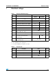
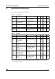
Table 5. On/off states
Symbol Parameter Test conditions Min. Typ. Max. Unit
V
(BR)DSS
Drain-source breakdown
voltage
I
D
= 1mA, V
GS
= 0 800 V
I
DSS
Zero gate voltage drain
current (V
GS
= 0)
V
DS
= Max rating,
V
DS
= Max rating,
Tc = 125°C
1
50
µA
µA
I
GSS
Gate body leakage current
(V
GS
= 0)
V
GS
= ± 20V ±10 µA
V
GS(th)
Gate threshold voltage V
DS
= V
GS
, I
D
= 100µA 3 3.75 4.5 V
R
DS(on)
Static drain-source on
resistance
V
GS
= 10V, I
D
= 2.15 A 1.9 2.4 Ω
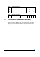
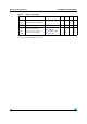
Table 6. Dynamic
Symbol Parameter Test conditions Min. Typ. Max. Unit
g
fs
(1)
1. Pulsed: pulse duration=300µs, duty cycle 1.5%
Forward transconductance V
DS
=15V, I
D
= 2.15A 4.25 S
C
iss
C
oss
C
rss
Input capacitance
Output capacitance
Reverse transfer
capacitance
V
DS
=25V, f=1 MHz, V
GS
=0
910
98
20
pF
pF
pF
C
osseq
(2)
.
2. C
oss eq.
is defined as a constant equivalent capacitance giving the same charging time as C
oss
when V
DS
increases from 0 to 80% V
DSS
Equivalent output
capacitance
V
GS
=0, V
DS
=0V to 400V 40 pF
t
d(on)
t
r
t
d(off)
t
r
Turn-on delay time
Rise time
Turn-on delay time
fall time
V
DD
=400 V, I
D
= 2 A,
R
G
=4.7Ω, V
GS
=10V
(see Figure 18)
18
25
45
30
ns
ns
ns
ns
Q
g
Q
gs
Q
gd
Total gate charge
Gate-source charge
Gate-drain charge
V
DD
=640V, I
D
= 4.3A
V
GS
=10V
32.4
5
18.5
45.5 nC
nC
nC
t
d(Voff)
t
r
Off-voltage rise time
Fall time
Cross-over time
V
DD
=640 V, I
D
= 4.3 A,
R
G
=4.7Ω, V
GS
=10V
(see Figure 20)
22
10
32
ns
ns
ns