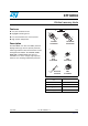
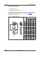
STTH4R02 Ultrafast recovery diode Features A ■ Very low conduction losses ■ Negligible switching losses ■ Low forward and reverse recovery times ■ High junction temperature K K A A K K TO-220AC STTH4R02D Description The STTH4R02 uses ST's new 200 V planar Pt doping technology, and it is specially suited for switching mode base drive and transistor circuits.
Characteristics 1 STTH4R02 Characteristics Table 2. Absolute ratings (limiting values at Tamb = 25 °C, unless otherwise stated) Symbol VRRM Parameter Repetitive peak reverse voltage Value Unit 200 V 70 A 4 A 70 A -65 to + 175 °C 175 °C Value Unit TO-220AC DPAK IF(RMS) Forward rms current SMB / SMC TO-220FPAC DO-201AB IF(AV) Average forward current, δ = 0.5 IFSM Surge non repetitive forward current Tstg Storage temperature range Tj Table 3.
STTH4R02 Table 4. Characteristics Static electrical characteristics Symbol Parameter IR(1) Test conditions Tj = 25 °C Reverse leakage current Tj = 125 °C Typ. Max. Unit 3 VR = VRRM µA 2 20 1.15 1.25 0.95 1.05 0.76 0.83 Typ. Max. IF = 1 A, dIF/dt = -50 A/µs, VR = 30 V, Tj = 25 °C 24 30 IF = 1 A, dIF/dt = -100 A/µs, VR = 30 V, Tj = 25 °C 16 20 Reverse recovery current IF = 4 A, dIF/dt = -200 A/µs, VR = 160 V, Tj = 125 °C 4.4 5.
Characteristics Figure 3. STTH4R02 Forward voltage drop versus forward current (maximum values) Figure 4. Relative variation of thermal impedance, junction to case, versus pulse duration Zth(j-c)/Rth(j-c) IFM(A) 1.0 100 Single pulse TO-220AC DPAK 90 80 70 60 Tj=150°C 50 Tj=25°C 40 30 20 10 VFM(V) tp(s) 0 0.1 0.0 0.5 Figure 5. 1.0 1.5 2.0 2.5 3.0 3.5 Relative variation of thermal impedance, junction to case, versus pulse duration 1.E-03 Figure 6. Zth(j-c)/Rth(j-c) 1.E-02 1.
STTH4R02 Figure 9. Characteristics Junction capacitance versus reverse applied voltage (typical values) Figure 10. Reverse recovery charges versus dIF/dt (typical values) C(pF) QRR(nC) 120 100 F=1MHz Vosc=30mVRMS Tj=25°C IF=4A VR=160V 100 Tj=125°C 80 60 40 Tj=25°C 20 VR(V) dIF/dt(A/µs) 10 0 1 10 100 1000 0 50 100 150 200 250 300 350 400 450 500 Figure 11. Reverse recovery time versus dIF/dt Figure 12.
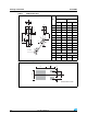
Ordering information scheme STTH4R02 Figure 15. Thermal resistance, junction to ambient, versus copper surface under tab - SMB Figure 16. Thermal resistance, junction to ambient, versus copper surface under tab - SMC Rth(j-a) (°C/W) Rth(j-a) (°C/W) 110 100 100 SMB Epoxy printed circuit board FR4, copper thickness = 35 µm 90 80 80 SMC Epoxy printed circuit board FR4, copper thickness = 35 µm 90 70 70 60 60 50 50 40 40 30 30 20 20 10 10 SCU(cm²) SCU(cm²) 0 0 0.0 0.5 1.0 1.
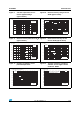
STTH4R02 3 Package information Package information ● Epoxy meets UL94, V0 ● Cooling method: by conduction (C) ● Recommended torque value: 0.4 to 0.6 N·m In order to meet environmental requirements, ST offers these devices in different grades of ECOPACK® packages, depending on their level of environmental compliance. ECOPACK® specifications, grade definitions and product status are available at: www.st.com. ECOPACK® is an ST trademark. Table 6. T0-220AC dimensions Dimensions Ref.
Package information Table 7. STTH4R02 DPAK dimensions Dimensions Ref. E C2 L2 Max Min. Max. A 2.20 2.40 0.086 0.094 A1 0.90 1.10 0.035 0.043 A2 0.03 0.23 0.001 0.009 B 0.64 0.90 0.025 0.035 D B2 5.20 5.40 0.204 0.212 C 0.45 0.60 0.017 0.023 C2 0.48 0.60 0.018 0.023 D 6.00 6.20 0.236 0.244 E 6.40 6.60 0.251 0.259 G 4.40 4.60 0.173 0.181 H 9.35 10.10 0.368 0.397 R H L4 A1 B R G Inches Min. A B2 Millimeters C A2 0.60 MIN. L2 V2 0.80 typ.
STTH4R02 Package information Table 8. T0-220FPAC dimensions Dimensions Ref. A B H Dia L6 L2 L7 L3 L5 F1 D F E Inches Min. Max. Min. Max. A 4.4 4.6 0.173 0.181 B 2.5 2.7 0.098 0.106 D 2.5 2.75 0.098 0.108 E 0.45 0.70 0.018 0.027 F 0.75 1 0.030 0.039 F1 1.15 1.70 0.045 0.067 G 4.95 5.20 0.195 0.205 G1 2.4 2.7 0.094 0.106 H 10 10.4 0.393 0.409 L2 L4 Millimeters 16 Typ. 0.63 Typ. L3 28.6 30.6 1.126 1.205 L4 9.8 10.6 0.386 0.417 L5 2.
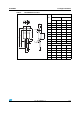
Package information Table 9. STTH4R02 SMB dimensions Dimensions Ref. Millimeters Inches E1 D Min. Max. Min. Max. A1 1.90 2.45 0.075 0.096 A2 0.05 0.20 0.002 0.008 b 1.95 2.20 0.077 0.087 c 0.15 0.40 0.006 0.016 D 3.30 3.95 0.130 0.156 E 5.10 5.60 0.201 0.220 E1 4.05 4.60 0.159 0.181 L 0.75 1.50 0.030 0.059 E A1 A2 C L b Figure 20. Footprint, dimensions in mm (inches) 1.62 2.60 (0.064) (0.102) 1.62 (0.064) 2.18 (0.086) 5.84 (0.
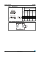
STTH4R02 Package information Table 10. SMC dimensions Dimensions Ref. Millimeters E1 D E Min. Max. Min. Max. A1 1.90 2.45 0.075 0.096 A2 0.05 0.20 0.002 0.008 (1) b 2.90 3.20 0.114 0.126 c(1) 0.15 0.40 0.006 0.016 D 5.55 6.25 0.218 0.246 E 7.75 8.15 0.305 0.321 E1 6.60 7.15 0.260 0.281 E2 4.40 4.70 0.173 0.185 L 0.75 1.50 0.030 0.059 A1 A2 C E2 L b Inches 1. Dimensions b and c apply to plated leads Figure 21.
Ordering information 4 Ordering information Table 12. 5 Ordering information Order code Marking Package Weight Base qty Delivery mode STTH4R02D STTH4R02 TO-220AC 1.86 g 50 Tube STTH4R02FP STTH4R02 TO-220FPAC 2.2 g 50 Tube STTH4R02B STTH4R02 DPAK 0.30 g 75 Tube STTH4R02B-TR STTH4R02 DPAK 0.30 g 2500 Tape and reel STTH4R02U 4R2U SMB 0.107 g 2500 Tape and reel STTH4R02 STTH4R02 DO-201AB 0.876 g 600 Ammopack STTH4R02RL STTH4R02 DO-201AB 0.
STTH4R02 Please Read Carefully: Information in this document is provided solely in connection with ST products. STMicroelectronics NV and its subsidiaries (“ST”) reserve the right to make changes, corrections, modifications or improvements, to this document, and the products and services described herein at any time, without notice. All ST products are sold pursuant to ST’s terms and conditions of sale.