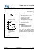
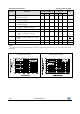
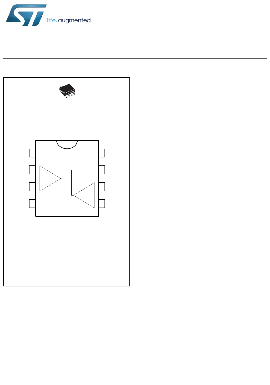
TL072, TL072A, TL072B Low noise JFET dual operational amplifiers Datasheet - production data Features • D SO8 Pin connections (top view) 1 8 2 - 3 + 4 7 Related products - 6 • • + 5 Description See TL071 for single op amp version See TL074 for quad op amp version The TL072, TL072A, and TL072B are high speed JFET input dual operational amplifiers incorporating well-matched, high-voltage JFET and bipolar transistors in a monolithic integrated circuit.
Contents TL072, TL072A, TL072B Contents 1 Schematic diagram.......................................................................... 3 2 Absolute maximum ratings and operating conditions ................. 4 3 4 Electrical characteristics ................................................................ 5 Parameter measurement information .......................................... 10 5 Typical application ........................................................................
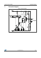
TL072, TL072A, TL072B 1 Schematic diagram Schematic diagram Figure 1: Schematic diagram DocID2298 Rev 8 3/16
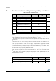
Absolute maximum ratings and operating conditions 2 TL072, TL072A, TL072B Absolute maximum ratings and operating conditions Table 1: Absolute maximum ratings Symbol VCC Vin Vid Parameter Supply voltage Input voltage TL072I, AI, BI (1) TL072C, AC, BC ±18 (2) Differential input voltage ±30 Thermal resistance junction to ambient, (4) SO8 125 Rthjc Thermal resistance junction to case, (4) SO8 40 Output short-circuit duration ESD V ±15 (3) Rthja Tstg Unit (5) Infinite Storage temperature
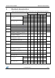
TL072, TL072A, TL072B 3 Electrical characteristics Electrical characteristics Table 3: Electrical characteristics at VCC = ±15 V, Tamb = +25 °C (unless otherwise specified). Symbol Parameter TL072I, AC, AI, BC, BI Min. Vio Input offset voltage (Rs = 50 Ω) Tamb = +25 °C Input offset voltage (Rs = 50 Ω) Tmin ≤ Tamb ≤ Tmax Typ. Max. TL072 3 10 TL072A 3 6 TL072B 1 3 TL072 13 TL072A 7 TL072B ΔVio/ΔT Iio (1) 5 Avd SVR ICC Max.
Electrical characteristics Symbol SR TL072, TL072A, TL072B Parameter TL072I, AC, AI, BC, BI Slew rate, Vin = 10 V, RL = 2 kΩ, CL = 100 pF, unity gain Min. Typ. 8 16 Max. TL072C Unit Min. Typ. Max. 8 16 V/µs tr Rise time, Vin = 20 mV, RL = 2 kΩ, CL = 100 pF, unity gain 0.1 0.1 µs Kov Overshoot, Vin = 20 mV, RL = 2 kΩ, CL = 100 pF, unity gain 10 10 % 4 MHz GBP Ri THD en Øm Vo1/Vo2 Gain bandwidth product, Vin = 10 mV, RL = 2 kΩ, CL = 100 pF, F= 100 kHz 2.5 4 2.5 12 Ω 0.
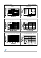
TL072, TL072A, TL072B Electrical characteristics Figure 4: Maximum peak-to-peak output voltage versus frequency Figure 5: Maximum peak-to-peak output voltage versus free air temperature Figure 6: Maximum peak-to-peak output voltage versus load resistance Figure 7: Maximum peak-to-peak output voltage versus supply voltage Figure 8: Input bias current versus free air temperature Figure 9: Large signal differential voltage amplification versus free air temperature DocID2298 Rev 8 7/16
Electrical characteristics TL072, TL072A, TL072B Figure 11: Total power dissipation versus free air temperature Figure 12: Supply current per amplifier versus free air temperature Figure 13: Common mode rejection ratio versus free air temperature SUPP LY CURREN T (mA) Figure 10: Large signal differential voltage amplification and phase shift versus frequency 2.0 1.8 1.6 1.4 1.2 1.0 0.8 0.6 0.4 0.
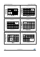
TL072, TL072A, TL072B Electrical characteristics Figure 16: Equivalent input noise voltage versus frequency Figure 17: Total harmonic distortion versus frequency DocID2298 Rev 8 9/16
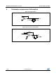
Parameter measurement information 4 TL072, TL072A, TL072B Parameter measurement information Figure 18: Voltage follower Figure 19: Gain-of-10 inverting amplifier 10/16 DocID2298 Rev 8
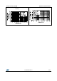
TL072, TL072A, TL072B 5 Typical application Typical application Figure 20: 100 kHz quadruple oscillator 1.
Package information 6 TL072, TL072A, TL072B Package information In order to meet environmental requirements, ST offers these devices in different grades of ECOPACK® packages, depending on their level of environmental compliance. ECOPACK® specifications, grade definitions and product status are available at: www.st.com. ECOPACK is an ST trademark. 6.
TL072, TL072A, TL072B Package information Table 4: SO8 package mechanical data Ref. Dimensions Millimeters Min. Typ. A Inches Max. Min. Typ. 1.75 0.069 A1 0.10 A2 1.25 b 0.28 0.48 0.011 0.019 c 0.17 0.23 0.007 0.010 D 4.80 4.90 5.00 0.189 0.193 0.197 E 5.80 6.00 6.20 0.228 0.236 0.244 E1 3.80 3.90 4.00 0.150 0.154 0.157 e 0.25 Max. 0.004 0.010 0.049 1.27 0.050 h 0.25 0.50 0.010 0.020 L 0.40 1.27 0.016 0.050 k 1° 8° 1° 8° ccc 0.
Ordering information 7 TL072, TL072A, TL072B Ordering information Table 5: Order codes Order code TL072IDT Temperature range Package Packing Marking -40 °C, +125 °C SΟ8 Tape and reel 072I TL072AIDT 072AI TL072BIDT 072BI TL072CDT 0 °C, +70 °C 072C TL072ACDT 072AC TL072BCDT 072BC TL072IYDT (1) -40 °C, +125 °C SO8 (automotive grade) 072IY TL072AIYDT (1) 072AIY TL072BIYDT (1) 072BIY Notes: (1) Qualified and characterized according to AEC Q100 and Q003 or equivalent, advanced
TL072, TL072A, TL072B 8 Revision history Revision history Table 6: Document revision history Date Revision Changes 28-Mar-2001 1 Initial release. 02-Apr-2004 2 Correction to pin connection diagram on cover page. Unpublished. 04-Dec-2006 3 Modified graphics in package mechanical data. 06-Mar-2007 4 Expanded order codes table and added automotive grade order codes. See Table 5: "Order codes". Added thermal resistance and ESD tolerance in Table 1: "Absolute maximum ratings".
TL072, TL072A, TL072B Please Read Carefully Information in this document is provided solely in connection with ST products. STMicroelectronics NV and its subsidiaries ("ST") reserve the right to make changes, corrections, modifications or improvements, to this document, and the products and services described herein at any time, without notice. All ST products are sold pursuant to ST’s terms and conditions of sale.