
Datasheet

VN5160S-E Block diagram and pins description
Doc ID 13493 Rev 5 5/31
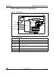
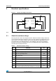
1 Block diagram and pins description
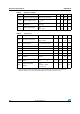
Figure 1. Block diagram
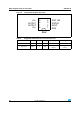
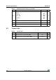
Table 2. Pins function
Name Function
V
CC
Battery connection.
OUTPUT Power output.
GND
Ground connection. Must be reverse battery protected by an external
diode/resistor network.
INPUT
Voltage controlled input pin with hysteresis, CMOS compatible. Controls output
switch state.
STATUS Open drain digital diagnostic pin.
STAT_DIS Active high CMOS compatible pin, to disable the STATUS pin.
LOGIC
UNDERVOLTAGE
OVERTEMP.
I
LIM
PwCLAMP
GND
INPUT
DRIVER
V
CC
CLAMP
V
DSLIM
STAT_DIS
STATUS
OPENLOAD ON
OPENLOAD OFF
Pwr
LIM
V
CC