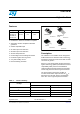
VN750-E High-side driver Datasheet − production data Features Type VN750-E VN750PT-E VN750B5-E VN750-12-E RDS(on) IOUT VCC 60 mΩ 6A 36 V 3(17$: $77 *$3*5, 3(17$:$77 LQ OLQH *$3*5, ■ ECOPACK®: lead free and RoHS compliant ■ Automotive Grade: compliance with AEC guidelines 3 3$. 33$ .
Contents VN750-E Contents 1 Block diagram and pin description . . . . . . . . . . . . . . . . . . . . . . . . . . . . . 5 2 Electrical specifications . . . . . . . . . . . . . . . . . . . . . . . . . . . . . . . . . . . . . . 6 3 4 2.1 Absolute maximum ratings . . . . . . . . . . . . . . . . . . . . . . . . . . . . . . . . . . . . . 6 2.2 Thermal data . . . . . . . . . . . . . . . . . . . . . . . . . . . . . . . . . . . . . . . . . . . . . . . 7 2.3 Electrical characteristics . . . . . . . . .
VN750-E List of tables List of tables Table 1. Table 2. Table 3. Table 4. Table 5. Table 6. Table 7. Table 8. Table 9. Table 10. Table 11. Table 12. Table 13. Table 14. Table 15. Table 16. Device summary . . . . . . . . . . . . . . . . . . . . . . . . . . . . . . . . . . . . . . . . . . . . . . . . . . . . . . . . . . 1 Suggested connections for unused and not connected pins . . . . . . . . . . . . . . . . . . . . . . . . 5 Absolute maximum ratings . . . . . . . . . . . . . . . . . . . . . . . . . . . .
List of figures VN750-E List of figures Figure 1. Figure 2. Figure 3. Figure 4. Figure 5. Figure 6. Figure 7. Figure 8. Figure 9. Figure 10. Figure 11. Figure 12. Figure 13. Figure 14. Figure 15. Figure 16. Figure 17. Figure 18. Figure 19. Figure 20. Figure 21. Figure 22. Figure 23. Figure 24. Figure 25. Figure 26. Figure 27. Figure 28. Figure 29. Figure 30. Figure 31. Figure 32. Figure 33. Figure 34. Figure 35. Figure 36. Figure 37. Figure 38. Figure 39. Figure 40. Figure 41. Figure 42. Figure 43.
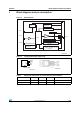
VN750-E 1 Block diagram and pin description Block diagram and pin description Figure 1. Block diagram 9 && 29(592/7$*( '(7(&7,21 9 & & &ODPS 81'(592/7$*( '(7(&7,21 *1' 3RZHU &/$03 '5,9(5 ,1387 287387 /2*,& &855(17 /,0,7(5 21 67$7( 23(1 /2$' '(7(&7,21 67$786 29(57(03(5$785( '(7(&7,21 2)) 67$7( 23(1 /2$' $1' 287387 6+257(' 72 9 && '(7(&7, 2 1 *$3*5, Figure 2. Configuration diagram (top view) 287387 67$786 9&& ,1387 *1' 33$. 3 3$.
Electrical specifications 2 VN750-E Electrical specifications Figure 3. Current and voltage conventions ,6 9) ,,1 ,1387 9&& ,67$7 ,287 67$786 9&& 287387 *1' 9,1 967$7 9287 ,*1' *$3*5, 2.1 Absolute maximum ratings Stress values that exceed those listed in the “Absolute maximum ratings” table can cause permanent damage to the device.
VN750-E Electrical specifications Table 3. Absolute maximum ratings (continued) Value Symbol Parameter PENTAWATT EMAX Ptot 138 138 mJ 60 W Internally limited °C Tj Junction operating temperature Tc Case operating temperature - 40 to 150 °C Storage temperature - 55 to 150 °C Tstg 2.2 PPAK Maximum switching energy (L=2.46 mH; RL=0 Ω; Vbat=13.5 V; Tjstart=150 °C; IL=9 A) Power dissipation TC=25°C Unit P2PAK Thermal data Table 4. Thermal data Max.
Electrical specifications Table 5. Electrical characteristics (continued) Symbol IS VN750-E Parameter Supply current Test conditions Min. Typ. Max. Unit 10 10 25 20 µA µA 2 3.5 mA 0 50 µA -75 0 µA Off-state; VCC=13 V; VIN=VOUT=0 V Off-state; VCC=13 V; VIN=VOUT=0 V; Tj=25 °C On-state; VCC=13 V; VIN=5 V; IOUT=0 A IL(off1) Off-state output current VIN=VOUT=0 V IL(off2) Off-state output current VIN=0V; VOUT=3.
VN750-E Table 5. Electrical specifications Electrical characteristics (continued) Symbol Parameter Test conditions Min. TR Reset temperature 135 Thyst Thermal hysteresis 7 tSDL Status delay in overload condition Tj>Tjsh Ilim Current limitation 9 V
Electrical specifications Figure 5. VN750-E Switching time waveforms 9287 G9287 GW RII G9287 GW RQ W 9,1 WG RQ WG RII W *$3*5, Table 6. Truth table Conditions Input Output Status Normal operation L H L H H H Current limitation L H H L X X H (Tj < TTSD) H (Tj > TTSD) L Over temperature L H L L H L Undervoltage L H L L X X Overvoltage L H L L H H Output voltage > VOL L H H H L H Output current < IOL L H L H H L Table 7.
VN750-E Electrical specifications Table 7. Electrical transient requirements on VCC pin (part 1/3) (continued) Test levels ISO T/R 7637/1 test pulse I II III IV Delays and impedance 3b +25 V +50 V +75 V +100 V 0.1 µs 50 Ω 4 -4 V -5 V -6 V -7 V 100 ms, 0.01 Ω 5 +26.5 V +46.5 V +66.5 V +86.5 V 400 ms, 2 Ω Table 8.
Electrical specifications Figure 6.
VN750-E 2.4 Electrical specifications Electrical characteristics curves Figure 7. Off-state output current Figure 8. High level input current Iih (uA) IL(off1) (uA) 7 3 2.5 6 Off state Vcc=36V Vin=Vout=0V 2 Vin=3.25V 5 1.5 4 1 3 0.5 2 0 1 -0.5 -1 0 -50 -25 0 25 50 75 100 125 150 175 -50 -25 0 25 Tc (ºC) Figure 9. 50 75 100 125 150 175 Tc (ºC) Input clamp voltage Figure 10. Status leakage current Ilstat (uA) Vicl (V) 8 0.05 7.8 Iin=1mA 0.04 7.6 Vstat=5V 7.
Electrical specifications VN750-E Figure 13. On-state resistance Vs Tcase Figure 14. On-state resistance Vs VCC Ron (mOhm) Ron (mOhm) 140 120 110 120 Iout=2A Iout=2A Vcc=8V; 13V; 36V 100 100 Tc= 150°C 90 80 80 Tc= 125°C 70 60 60 50 40 Tc= 25°C 40 Tc= - 40°C 20 30 0 20 -50 -25 0 25 50 75 100 125 150 175 5 10 15 20 Tc (ºC) 25 30 35 40 Vcc (V) Figure 15. Open-load on-state detection Figure 16. Input high level threshold Iol (mA) Vih (V) 220 3.6 200 3.
VN750-E Electrical specifications Figure 19. Overvoltage shutdown Figure 20. Open-load off-state voltage detection threshold Vol (V) Vov (V) 5 50 48 4.5 Vin=0V 46 4 44 3.5 42 40 3 38 2.5 36 2 34 1.5 32 30 1 -50 -25 0 25 50 75 100 125 150 175 -50 -25 0 25 Tc (°C) 50 75 100 125 150 175 Tc (ºC) Figure 21. Turn-on voltage slope Figure 22. Turn-off voltage slope dVout/dt/(on) (V/ms) dVout/dt(off) (V/ms) 1000 500 900 450 Vcc=13V Rl=6.5Ohm 800 Vcc=13V Rl=6.
Electrical specifications VN750-E Figure 24. Application schematic 9 9 9 && 5 SURW 67$786 ' OG & 5 SURW ,1387 287387 *1' 9 *1' 5 *1' ' *1' *$3*5, 2.5 GND protection network against reverse battery 2.5.1 Solution 1: resistor in the ground line (RGND only) This can be used with any type of load. The following is an indication on how to size the RGND resistor. 1. RGND ≤ 600mV / (IS(on)max). 2.
VN750-E 2.5.2 Electrical specifications Solution 2: diode (DGND) in the ground line A resistor (RGND=1 kΩ) should be inserted in parallel to DGND if the device drives an inductive load. This small signal diode can be safely shared amongst several different HSDs. Also in this case, the presence of the ground network produces a shift (≈600mV) in the input threshold and in the status output values if the microprocessor ground is not common to the device ground.
Electrical specifications VN750-E Because Is(OFF) may significantly increase if Vout is pulled high (up to several mA), the pullup resistor RPU should be connected to a supply that is switched off when the module is in standby. The values of VOLmin, VOLmax and IL(off2) are available in the electrical characteristics section. Figure 25. Open-load detection in off-state V batt.
VN750-E 2.9 Electrical specifications PPAK/P2PAK maximum demagnetization energy (VCC=13.5V) Figure 26.
Package and PCB thermal data VN750-E 3 Package and PCB thermal data 3.1 P2PAK thermal data Figure 27. P2PAK PC board GAPGRI00194 Note: Layout condition of Rth and Zth measurements (PCB FR4 area = 60 mm x 60 mm, PCB thickness = 2 mm, Cu thickness=35 µm, Copper areas: 0.97 cm2, 8 cm2). Figure 28. P2PAK Rthj-amb Vs.
VN750-E Package and PCB thermal data Figure 29. P2PAK thermal impedance junction ambient single pulse =7+ & : FP FP FP 7LPH V *$3*5, Equation 1: pulse calculation formula Z THδ = R TH ⋅δ+Z THtp (1 – δ) where δ = tP/T Figure 30.
Package and PCB thermal data Table 10. 3.2 VN750-E P2PAK thermal parameter Area/island (cm2) 0.5 R1 (°C/W) 0.15 R2 (°C/W) 0.7 R3 (°C/W) 0.7 R4 (°C/W) 4 R5 (°C/W) 9 R6 (°C/W) 37 C1 (W·s/°C) 0.0006 C2 (W·s/°C) 0.0025 C3 (W·s/°C) 0.055 C4 (W·s/°C) 0.4 C5 (W·s/°C) 2 C6 (W·s/°C) 3 6 22 5 PPAK thermal data Figure 31.
VN750-E Package and PCB thermal data Figure 32. PPAK Rthj-amb Vs. PCB copper area in open box free air condition 57+MBDPE & : 3&% &X KHDWVLQN DUHD FPA *$3*5, Figure 33.
Package and PCB thermal data VN750-E Equation 2: pulse calculation formula Z THδ = R TH ⋅δ+Z THtp (1 – δ) where δ = tP/T Figure 34. PPAK thermal fitting model of a single channel GAPGRI00200 Table 11. 24/38 PPAK thermal parameter Area/island (cm2) 0.5 R1 (°C/W) 0.15 R2 (°C/W) 0.7 R3 (°C/W) 1.6 R4 (°C/W) 2 R5 (°C/W) 15 R6 (°C/W) 61 C1 (W·s/°C) 0.0006 C2 (W·s/°C) 0.0025 C3 (W·s/°C) 0.08 C4 (W·s/°C) 0.3 C5 (W·s/°C) 0.45 C6 (W·s/°C) 0.
VN750-E Package and packing information 4 Package and packing information 4.1 ECOPACK® packages In order to meet environmental requirements, ST offers these devices in different grades of ECOPACK® packages, depending on their level of environmental compliance. ECOPACK® specifications, grade definitions and product status are available at: www.st.com. ECOPACK® is an ST trademark. 4.2 PENTAWATT mechanical data Figure 35. PENTAWATT package dimensions Table 12. PENTAWATT mechanical data mm Dim. Min.
Package and packing information Table 12. VN750-E PENTAWATT mechanical data (continued) mm Dim. Min. Typ. D1 1.2 1.35 E 0.35 0.55 F 0.8 1.05 F1 1 1.4 G 3.2 3.4 3.6 G1 6.6 6.8 7 H2 H3 10.4 10.05 10.4 L 17.85 L1 15.75 L2 21.4 L3 22.5 L5 2.6 3 L6 15.1 15.8 L7 6 6.6 M 4.5 M1 4 Diam. 26/38 Max. 3.65 Doc ID 10891 Rev 7 3.
VN750-E 4.2.1 Package and packing information PENTAWATT (in-line) mechanical data Figure 36. PENTAWATT (in-line) package dimensions Table 13. PENTAWATT (in-line) mechanical data millimeters Symbol Min Typ Max A 4.3 4.8 C 1.17 1.37 D 2.4 2.8 E 0.35 0.55 F 0.8 1.05 F2 1.1 1.4 F3 1.25 1.55 G 3.2 3.6 G1 6.6 7 H1 9.3 9.7 H2 10.4 H3 10.05 10.4 L2 23.05 23.8 L3 25.3 26.
Package and packing information Table 13. VN750-E PENTAWATT (in-line) mechanical data (continued) millimeters Symbol Min Max L4 0.9 2.9 L5 2.6 3 L6 15.1 15.8 L7 6 6.6 V4 Diam. 28/38 Typ 90° 3.65 Doc ID 10891 Rev 7 3.
VN750-E 4.3 Package and packing information P2PAK mechanical data Figure 37.
Package and packing information VN750-E P2PAK mechanical data Table 14. mm Dim. Min. Max. A 4.30 4.80 A1 2.40 2.80 A2 0.03 0.23 b 0.80 1.05 c 0.45 0.60 c2 1.17 1.37 D 8.95 9.35 D2 E 8.00 10.00 E1 10.40 8.50 e 3.20 3.60 e1 6.60 7.00 L 13.70 14.50 L2 1.25 1.40 L3 0.90 1.70 L5 1.55 2.40 0.40 R V2 0º Package weight 30/38 Typ. 8º 1.40 Gr.
VN750-E 4.4 Package and packing information PPAK mechanical data Figure 38.
Package and packing information Table 15. VN750-E PPAK mechanical data mm Dim. Min. Max. A 2.20 2.40 A1 0.90 1.10 A2 0.03 0.23 B 0.40 0.60 B2 5.20 5.40 C 0.45 0.60 C2 0.48 0.60 D1 5.1 D 6.00 6.20 E 6.40 6.60 E1 4.7 e 1.27 G 4.90 5.25 G1 2.38 2.70 H 9.35 10.10 L2 0.8 L4 0.60 L5 1 2.80 R 0.2 0º Package weight 8º Gr. 0.3 Doc ID 10891 Rev 7 1.00 1.00 L6 V2 32/38 Typ.
VN750-E 4.5 Package and packing information PENTAWATT packing information The devices can be packed in tube or tape and reel shipments (see the Device summary on page 1). Figure 39. PENTAWATT tube shipment (no suffix) %DVH 4 W\ %XON 4 W\ 7XEH OHQJWK $ % & % & $OO GLPHQVLRQV DUH LQ PP $ *$3*5, 4.6 P2PAK packing information The devices can be packed in tube or tape and reel shipments (see the Device summary on page 1). Figure 40.
Package and packing information VN750-E Figure 41. P2PAK tape and reel (suffix “13TR”) REEL DIMENSIONS All dimensions are in mm. Base Q.ty Bulk Q.ty A (max) B (min) C (± 0.2) F G (+ 2 / -0) N (min) T (max) 1000 1000 330 1.5 13 20.2 24.4 60 30.4 TAPE DIMENSIONS According to Electronic Industries Association (EIA) Standard 481 rev. A, Feb 1986 Tape width Tape Hole Spacing Component Spacing Hole Diameter Hole Diameter Hole Position Compartment Depth Hole Spacing All dimensions are in mm. W P0 (± 0.
VN750-E 4.7 Package and packing information PPAK packing information The devices can be packed in tube or tape and reel shipments (see the Device summary on page 1). Figure 42. PPAK suggested pad layout *$3*5, Figure 43. PPAK tube shipment (no suffix) $ & % Base Q.ty 75 Bulk Q.ty 3000 Tube length (± 0.5) 532 A 6 B 21.3 C (± 0.1) 0.6 *$3*5, All dimensions are in mm.
Package and packing information VN750-E Figure 44. PPAK tape and reel REEL DIMENSIONS All dimensions are in mm. Base Q.ty Bulk Q.ty A (max) B (min) C (± 0.2) F G (+ 2 / -0) N (min) T (max) 2500 2500 330 1.5 13 20.2 16.4 60 22.4 TAPE DIMENSIONS According to Electronic Industries Association (EIA) Standard 481 rev. A, Feb 1986 Tape width Tape Hole Spacing Component Spacing Hole Diameter Hole Diameter Hole Position Compartment Depth Hole Spacing W P0 (± 0.1) P D (± 0.1/-0) D1 (min) F (± 0.
VN750-E 5 Revision history Revision history Table 16. Document revision history Date Revision 07-Oct-2004 1 Initial release. 2 Document reformatted and restructured. Added content, list of figures and tables. Added ECOPACK® packages information. Updated Figure 41: P2PAK tape and reel (suffix “13TR”): – changed component spacing (P) in tape dimensions table from 16 mm to 12 mm. 3 Removed SO-8 package into the following tables: Table 1, Table 3 and Table 4.
VN750-E Please Read Carefully: Information in this document is provided solely in connection with ST products. STMicroelectronics NV and its subsidiaries (“ST”) reserve the right to make changes, corrections, modifications or improvements, to this document, and the products and services described herein at any time, without notice. All ST products are sold pursuant to ST’s terms and conditions of sale.