
Datasheet


VN750-E Block diagram and pin description
Doc ID 10891 Rev 7 5/38
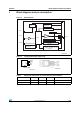
1 Block diagram and pin description
Figure 1. Block diagram
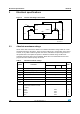
Figure 2. Configuration diagram (top view)
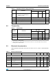
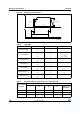
Table 2. Suggested connections for unused and not connected pins
Connection/pin Status N.C. Output Input
Floating X X X X
To ground X Through 10 KΩ resistor
81'(592/7$*(
9
&&
*1'
,1387
287387
&855(17 /,0 ,7(5
/2*,&
'5,9(5
3RZHU &/$03
67$786
9
& &
21 67$7( 23(1/2$'
2)) 67$7( 23(1/2$'
$1' 287387 6+257(' 72 9
&&
'(7(&7,21
'(7(&7,21
'(7(&7,21
*$3*5,
&ODPS
29(592/7$*(
'(7(&7,21
29(57(03(5$785(
'(7(&7,21
287387
67$786
9
&&
,1387
*1'
33$.3
3$.
*$3*5,
3(17$:$77
*$3*5,