VN920SP-E High-side driver Features Type RDS(on) IOUT VCC VN920SP-E 15 mΩ 30 A 36 V ■ ECOPACK®: lead free and RoHS compliant ■ Automotive Grade: compliance with AEC guidelines ■ Very low standby current ■ CMOS compatible input ■ Proportional load current sense ■ Current sense disable ■ Thermal shutdown protection and diagnosis ■ Undervoltage shutdown ■ Overvoltage clamp ■ Load current limitation Description The VN920SP-E is a monolithic device designed in STMicroelectronics™ VIPo
Contents VN920SP-E Contents 1 Block diagram and pin description . . . . . . . . . . . . . . . . . . . . . . . . . . . . . 5 2 Electrical specifications . . . . . . . . . . . . . . . . . . . . . . . . . . . . . . . . . . . . . . 6 3 2.1 Absolute maximum ratings . . . . . . . . . . . . . . . . . . . . . . . . . . . . . . . . . . . . . 6 2.2 Thermal data . . . . . . . . . . . . . . . . . . . . . . . . . . . . . . . . . . . . . . . . . . . . . . . 7 2.3 Electrical characteristics . . . . . . . . . .
VN920SP-E List of tables List of tables Table 1. Table 2. Table 3. Table 4. Table 5. Table 6. Table 7. Table 8. Table 9. Table 10. Table 11. Table 12. Table 13. Table 14. Table 15. Table 16. Table 17. Device summary . . . . . . . . . . . . . . . . . . . . . . . . . . . . . . . . . . . . . . . . . . . . . . . . . . . . . . . . . . 1 Suggested connections for unused and not connected pins . . . . . . . . . . . . . . . . . . . . . . . . 5 Absolute maximum ratings . . . . . . . . . . . . . . . . . . . . . .
List of figures VN920SP-E List of figures Figure 1. Figure 2. Figure 3. Figure 4. Figure 5. Figure 6. Figure 7. Figure 8. Figure 9. Figure 10. Figure 11. Figure 12. Figure 13. Figure 14. Figure 15. Figure 16. Figure 17. Figure 18. Figure 19. Figure 20. Figure 21. Figure 22. Figure 23. Figure 24. Figure 25. Figure 26. Figure 27. 4/27 Block diagram . . . . . . . . . . . . . . . . . . . . . . . . . . . . . . . . . . . . . . . . . . . . . . . . . . . . . . . . . . . . 5 Configuration diagram (top view) . .
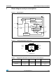
VN920SP-E 1 Block diagram and pin description Block diagram and pin description Figure 1. Block diagram VCC OVERVOLTAGE DETECTION VCC CLAMP UNDERVOLTAGE DETECTION GND Power CLAMP DRIVER OUTPUT LOGIC INPUT CURRENT LIMITER VDS LIMITER IOUT CURRENT SENSE K OVERTEMPERATURE DETECTION Figure 2. Configuration diagram (top view) GROUND INPUT C.SENSE N.C. N.C. 6 5 OUTPUT 7 4 8 3 OUTPUT N.C. 9 2 OUTPUT 10 1 OUTPUT 11 VCC PowerSO-10 Table 2.
Electrical specifications 2 VN920SP-E Electrical specifications Figure 3. Current and voltage conventions IS VCC VF VCC IOUT OUTPUT IIN VOUT INPUT VIN ISENSE CURRENT SENSE VSENSE GND IGND 2.1 Absolute maximum ratings Stressing the device above the rating listed in Table 3 may cause permanent damage to the device. These are stress ratings only and operation of the device at these or any other conditions above those indicated in the operating sections of this specification is not implied.
VN920SP-E Electrical specifications Table 3. Absolute maximum ratings (continued) Symbol Value Unit Maximum switching energy (L = 0.25 mH; RL= 0 Ω; Vbat = 13.5 V; Tjstart = 150 °C; IL = 45 A) 362 mJ Ptot Power dissipation TC ≤ 25 °C 96.1 W Tj Junction operating temperature Internally limited °C Tc Case operating temperature -40 to 150 °C Storage temperature -55 to 150 °C EMAX TSTG 2.2 Parameter Thermal data Table 4.
Electrical specifications 2.3 VN920SP-E Electrical characteristics Values specified in this section are for 8 V < VCC < 36 V; -40 °C < Tj < 150 °C, unless otherwise stated. Table 5. Power Symbol Parameter VCC Test conditions Min. Typ. Operating supply voltage 5.5 13 36 V VUSD Undervoltage shutdown 3 4 5.
VN920SP-E Electrical specifications Table 7. Symbol Logic inputs Parameter Test conditions VIL Input low level voltage IIL Low level input current VIH Input high level voltage IIH High level input current VI(hyst) Input hysteresis voltage VICL Table 8. Typ. Max. Unit 1.25 V 1 µA 3.25 V VIN = 3.25 V 10 0.5 µA V 6 6.8 -0.7 8 V V Min. Typ. Max. Unit - - 0.6 V VCC output diode Parameter VF Forward on voltage Symbol VIN = 1.
Electrical specifications VN920SP-E Table 10. Current sense(1) Symbol Parameter Test conditions Typ. Max. 4400 6000 IOUT/ISENSE IOUT = 1 A; VSENSE = 0.5 V; Tj = -40 °C...150 °C 3300 Current sense ratio drift IOUT = 1 A; VSENSE = 0.5 V; Tj = - 40 °C...150 °C -10 IOUT/ISENSE IOUT = 10 A; VSENSE = 4 V; Tj = - 40 °C Tj = 25 °C...150 °C Current sense ratio drift IOUT = 10 A; VSENSE = 4 V; Tj = -40 °C...150 °C IOUT/ISENSE IOUT = 30 A; VSENSE = 4 V; Tj = -40 °C Tj = 25 °C...
VN920SP-E Electrical specifications Table 11.
Electrical specifications Table 12. VN920SP-E Electrical transient requirements on VCC pin (part 1) ISO T/R Test levels 7637/1 test pulse I II III IV Delays and impedance 1 - 25V - 50 V - 75 V - 100 V 2 ms, 10 Ω 2 + 25 V + 50 V + 75V + 100V 0.2 ms, 10 Ω 3a - 25 V - 50 V - 100 V - 150 V 0.1 µs, 50 Ω 3b + 25 V + 50 V + 75 V + 100 V 0.1 µs, 50 Ω 4 -4V -5V -6V -7V 100 ms, 0.01 Ω 5 + 26.5 V + 46.5 V + 66.5 V + 86.5 V 400 ms, 2 Ω Table 13.
VN920SP-E Electrical specifications Figure 4. Switching characteristics (resistive load RL= 1.3 Ω) VOUT 90% 80% dVOUT/dt(off) dVOUT/dt(on) 10% tr tf t ISENSE 90% t tDSENSE INPUT td(on) td(off) t Figure 5. IOUT/ISENSE versus IOUT IOUT/ISENSE 6500 6500 6000 6000 max.Tj=-40°C 5500 5500 max.Tj=25...150°C 5000 5000 typical value min.Tj=25...150°C 4500 4500 min.
Electrical specifications Figure 6.
VN920SP-E Electrical specifications 2.4 Electrical characteristics curves Figure 7. Off-state output current Figure 8. High level input current Iih (uA) IL(off1) (uA) 5 9 4.5 8 Vin=3.25V 4 7 3.5 6 3 5 2.5 4 2 3 1.5 2 1 1 0.5 0 0 -50 -25 0 25 50 75 100 125 150 -50 175 -25 0 25 Figure 9. 50 75 100 125 150 175 Tc (°C) Tc (°C) Input clamp voltage Figure 10. On-state resistance vs VCC Ron (mOhm) Vicl (V) 30 8 Tc= 150ºC 27.5 7.8 25 Iin=1mA 7.6 22.5 7.
Electrical specifications VN920SP-E Figure 13. Input low level Figure 14. Input hysteresis voltage Vil (V) Vhyst (V) 2.6 1.5 1.4 2.4 1.3 2.2 1.2 2 1.1 1.8 1 0.9 1.6 0.8 1.4 0.7 1.2 0.6 1 0.5 -50 -25 0 25 50 75 100 125 150 175 -50 -25 0 25 50 Tc (°C) 75 100 125 150 175 Tc (°C) Figure 15. Turn-on voltage slope Figure 16. Turn-off voltage slope dVout/dt(on) (V/ms) dVout/dt(off) (V/ms) 700 550 500 650 Vcc=13V Rl=1.3Ohm 450 Vcc=13V Rl=1.
VN920SP-E 3 Application information Application information Figure 19. Application schematic +5V VCC Rprot INPUT Dld μC Rprot OUTPUT CURRENT SENSE RSENSE GND VGND RGND DGND 3.1 GND protection network against reverse battery 3.1.1 Solution 1: resistor in the ground line (RGND only) This can be used with any type of load. The following is an indication on how to dimension the RGND resistor. 1. RGND ≤ 600 mV / (IS(on)max) 2.
Application information 3.1.2 VN920SP-E Solution 2: diode (DGND) in the ground line A resistor (RGND = 1 kΩ) should be inserted in parallel to DGND if the device drives an inductive load. This small signal diode can be safely shared amongst several different HSDs. Also in this case, the presence of the ground network produces a shift (∼600mV) in the input threshold and in the status output values if the microprocessor ground is not common to the device ground.
VN920SP-E 3.4 Application information PowerSO-10 maximum demagnetization energy (VCC = 13.5 V) Figure 20. PowerSO-10 maximum turn-off current versus inductance I LM AX (A) 100 A 10 B C 1 0,01 0,1 1 10 100 L(mH) A: Tjstart = 150 °C single pulse B: Tjstart = 100 °C repetitive pulse C: Tjstart = 125 °C repetitive pulse VIN, IL Demagnetization Demagnetization Demagnetization t Note: Values are generated with RL = 0 Ω.
Package and PCB thermal data VN920SP-E 4 Package and PCB thermal data 4.1 PowerSO-10 thermal data Figure 21. PowerSO-10 PC board Note: Layout condition of Rth and Zth measurements (PCB FR4 area = 58 mm x 58 mm, PCB thickness = 2 mm, Cu thickness = 35 µm, Copper areas: from minimum pad layout to 8 cm2). Figure 22.
VN920SP-E Package and PCB thermal data Figure 23. PowerSO-10 thermal impedance junction ambient single pulse Equation 1: pulse calculation formula Z THδ = R TH ⋅ δ + Z THtp ( 1 – δ ) where δ = tp ⁄ T Figure 24.
Package and PCB thermal data Table 15. 22/27 VN920SP-E Thermal parameters Area / island (cm2) Footprint R1 (°C/W) 0.02 R2 (°C/W) 0.1 R3 (°C/W) 0.2 R4 (°C/W) 0.8 R5 (°C/W) 12 R6 (°C/W) 37 C1 (W.s/°C) 0.0015 C2 (W.s/°C) 7.00E-03 C3 (W.s/°C) 0.015 C4 (W.s/°C) 0.3 C5 (W.s/°C) 0.75 C6 (W.
VN920SP-E Package and packing information 5 Package and packing information 5.1 ECOPACK® packages In order to meet environmental requirements, ST offers these devices in different grades of ECOPACK® packages, depending on their level of environmental compliance. ECOPACK® specifications, grade definitions and product status are available at: www.st.com. ECOPACK® is an ST trademark. 5.2 PowerSO-10 mechanical data Figure 25.
Package and packing information Table 16. VN920SP-E PowerSO-10 mechanical data Millimeters Dim. Min. Max. A 3.35 3.65 A(1) 3.4 3.6 A1 0.00 0.10 B 0.40 0.60 B(1) 0.37 0.53 C 0.35 0.55 C(1) 0.23 0.32 D 9.40 9.60 D1 7.40 7.60 E 9.30 9.50 E2 7.20 7.60 E2(1) 7.30 7.50 E4 5.90 6.10 E4(1) 5.90 6.30 e 1.27 F 1.25 1.35 F(1) 1.20 1.40 H 13.80 14.40 H(1) 13.85 14.35 h 0.50 L 1.20 1.80 L(1) 0.80 1.10 a 0° 8° α(1) 2° 8° 1. Muar only POA P013P.
VN920SP-E Package and packing information 5.3 PowerSO-10 packing information Figure 26. PowerSO-10 suggested pad layout and tube shipment (no suffix) Figure 27. PowerSO-10 tape and reel shipment (suffix “TR”) Reel dimensions Base Q.ty Bulk Q.ty A (max) B (min) C (± 0.2) F G (+ 2 / -0) N (min) T (max) 600 600 330 1.5 13 20.2 24.4 60 30.4 Tape dimensions According to Electronic Industries Association (EIA) Standard 481 rev. A, Feb.
Revision history 6 VN920SP-E Revision history Table 17. 26/27 Document revision history Date Revision Changes 01-Oct-2004 1 Initial release. 17-May-2010 2 Updated Features list. 07-Feb-2011 3 Updated Table 6: Switching (VCC = 13 V) 19-Sep-2013 4 Updated Disclaimer.
VN920SP-E Please Read Carefully: Information in this document is provided solely in connection with ST products. STMicroelectronics NV and its subsidiaries (“ST”) reserve the right to make changes, corrections, modifications or improvements, to this document, and the products and services described herein at any time, without notice. All ST products are sold pursuant to ST’s terms and conditions of sale.