
Datasheet


VN920SP-E Block diagram and pin description
Doc ID 10896 Rev 4 5/27
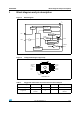
1 Block diagram and pin description
Figure 1. Block diagram
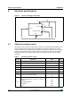
Figure 2. Configuration diagram (top view)
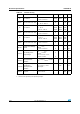
Table 2. Suggested connections for unused and not connected pins
Connection / pin Current sense N.C. Output Input
Floating X X X
To ground
Through 1 KΩ
resistor
X
Through 10KΩ
resistor
UNDERVOLTAGE
OVERTEMPERATURE
V
CC
GND
INPUT
OUTPUT
OVERVOLTAGE
CURRENT
LIMITER
LOGIC
DRIVER
Power
CLAMP
V
CC
CLAMP
V
DS
LIMITER
DETECTION
DETECTION
DETECTION
K
I
OUT
CURRENT
SENSE
1
2
3
4
5
6
7
8
9
10
11
OUTPUT
OUTPUT
OUTPUT
OUTPUT
GROUND
INPUT
C.SENSE
N.C.
N.C.
V
CC
N.C.
PowerSO-10