VNS1NV04DP-E OMNIFET II fully autoprotected Power MOSFET Features Max On-state resistance(1) RDS(ON) 250m (1) Current limitation (typ) (1) Drain-Source clamp voltage ILIMH 1.7A VCLAMP 40V 1. Per each device.
Contents VNS1NV04DP-E Contents 1 Block diagram and pin description . . . . . . . . . . . . . . . . . . . . . . . . . . . . . 5 2 Electrical specifications . . . . . . . . . . . . . . . . . . . . . . . . . . . . . . . . . . . . . . 6 3 4 2.1 Absolute maximum ratings . . . . . . . . . . . . . . . . . . . . . . . . . . . . . . . . . . . . . 6 2.2 Thermal data . . . . . . . . . . . . . . . . . . . . . . . . . . . . . . . . . . . . . . . . . . . . . . . 7 2.3 Electrical characteristics . . . . . . .
VNS1NV04DP-E List of tables List of tables Table 1. Table 2. Table 3. Table 4. Table 5. Table 6. Table 7. Table 8. Table 9. Table 10. Table 11. Table 12. Device summary . . . . . . . . . . . . . . . . . . . . . . . . . . . . . . . . . . . . . . . . . . . . . . . . . . . . . . . . . . 1 Absolute maximum ratings . . . . . . . . . . . . . . . . . . . . . . . . . . . . . . . . . . . . . . . . . . . . . . . . . . 6 Thermal data. . . . . . . . . . . . . . . . . . . . . . . . . . . . . . . . . . . . . . . . . .
List of figures VNS1NV04DP-E List of figures Figure 1. Figure 2. Figure 3. Figure 4. Figure 5. Figure 6. Figure 7. Figure 8. Figure 9. Figure 10. Figure 11. Figure 12. Figure 13. Figure 14. Figure 15. Figure 16. Figure 17. Figure 18. Figure 19. Figure 20. Figure 21. Figure 22. Figure 23. Figure 24. Figure 25. Figure 26. Figure 27. Figure 28. Figure 29. Figure 30. Figure 31. Figure 32. Figure 33. Figure 34. Figure 35. Figure 36. 4/24 Block diagram . . . . . . . . . . . . . . . . . . . . . . . . . . . . .
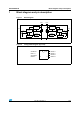
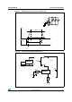
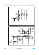
VNS1NV04DP-E 1 Block diagram and pin description Block diagram and pin description Figure 1. Block diagram DRAIN2 DRAIN1 OVERVOLTAGE CLAMP OVERVOLTAGE CLAMP INPUT1 GATE CONTROL GATE CONTROL OVER TEMPERATURE LINEAR CURRENT LIMITER LINEAR CURRENT LIMITER SOURCE1 Figure 2.
Electrical specifications 2 VNS1NV04DP-E Electrical specifications Figure 3. Current and voltage conventions RIN1 IIN1 ID1 INPUT 1 VIN1 IIN2 DRAIN 1 RIN2 ID2 INPUT 2 VIN2 2.1 SOURCE 1 VDS1 DRAIN 2 VDS1 SOURCE 2 Absolute maximum ratings Stressing the device above the rating listed in the “Absolute maximum ratings” table may cause permanent damage to the device.
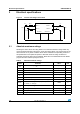
VNS1NV04DP-E 2.2 Electrical specifications Thermal data Table 3. Thermal data Symbol 2.3 Parameter Rthj-lead Thermal resistance junction-lead (per channel) Rthj-amb Thermal resistance junction-ambient Max. value Unit 30 °C/W See Figure 31 °C/W Electrical characteristics Table 4. Symbol Off(1) Parameter Test conditions Min. Typ. Max. Unit 45 55 V VCLAMP Drain-source clamp voltage VIN = 0 V; ID = 0.
Electrical specifications VNS1NV04DP-E Table 7. Switching(1) Symbol Parameter td(on) Test conditions Turn-on delay time VDD = 15 V; ID = 0.5 A; Vgen = 5 V; Rgen = RIN MIN = 330 (see Figure 4) Rise time tr td(off) tf Min. Turn-off delay time Fall time td(on) Turn-on delay time VDD = 15 V; ID = 0.5 A Vgen = 5 V; Rgen = 2.2 K (see Figure 4) Rise time tr td(off) Turn-off delay time Fall time tf (dI/dt)on Qi Typ. Max. Unit 70 200 ns 170 500 ns 350 1000 ns 200 600 ns 0.
VNS1NV04DP-E Figure 4. Electrical specifications Switching time test circuit for resistive load VD Rgen Vgen ID 90% tr tf 10% t td(on) Vgen td(off) t Figure 5. Test circuit for diode recovery times A A D I FAST DIODE OMNIFET S L=100uH B B 330 D Rgen I Vgen VDD OMNIFET S 8.
Electrical specifications Figure 6. VNS1NV04DP-E Unclamped inductive load test circuits RGEN VIN PW Figure 7.
VNS1NV04DP-E Figure 8.
Electrical specifications 2.4 VNS1NV04DP-E Electrical characteristics curves Figure 9. Source-drain diode forward characteristics Figure 10. Static drain-source on resistance Vsd (mV) Rds(on) (ohms) 1000 4.5 Tj=-40ºC 4 950 Vin=2.5V 3.5 Vin=0V 900 3 2.5 850 2 800 1.5 Tj=25ºC 1 750 Tj=150ºC 0.5 700 0 0 2 4 6 8 10 12 14 0 0.05 0.1 Id (A) Figure 11. 0.15 0.2 0.25 0.3 Id(A) Derating curve Figure 12.
VNS1NV04DP-E Electrical specifications Figure 15. Static drain-source on resistance vs id Figure 16. Transfer characteristics Rds(on) (mohms) Idon(A) 500 2.25 Vin=3.5V 450 Tj=25ºC 2 Tj=150ºC 400 Vds=13.5V 1.75 Vin=5V 350 1.5 300 1.25 250 Vin=3.5V 1 Vin=5V Vin=3.5V 0.75 Tj=150ºC Tj=25ºC 200 150 Tj=-40ºC 0.5 Tj=-40ºC Vin=5V 100 0.25 50 0 1.5 0 0 0.25 0.5 0.75 1 1.25 1.5 1.75 2 1.75 2 2.5 2.25 3 2.75 4 4.5 3.75 4.25 5 4.75 Vin(V) Id(A) Figure 17.
Electrical specifications VNS1NV04DP-E Figure 21. Turn-off drain-source voltage Figure 22. Capacitance variations slope (part 2/2) dv/dt(V/us) C(pF) 350 225 200 300 Vin=3.5V Vdd=15V Id=0.5A 250 f=1MHz Vin=0V 175 200 150 150 125 100 100 50 75 50 0 0 500 1000 1500 2000 0 2500 5 10 15 20 25 30 35 Vds(V) Rg(ohm) Figure 23. Switching time resistive load Figure 24. Switching time resistive load (part 1/2) (part 2/2) t(ns) t(us) 550 2 500 1.75 td(off) Vdd=15V Id=0.
VNS1NV04DP-E Electrical specifications Figure 27. Normalized input threshold voltage vs temperature Figure 28. Normalized current limit vs junction temperature Vinth (V) Ilim (A) 2 5 1.8 4.5 Vds=Vin Id=1mA 1.6 Vin=5V Vds=13V 4 1.4 3.5 1.2 3 1 2.5 0.8 2 0.6 1.5 0.4 1 0.2 0.5 0 0 -50 -25 0 25 50 75 100 125 150 175 Tc (ºC) -50 -25 0 25 50 75 100 125 150 175 Tc (ºC) Figure 29. Step response current limit Tdlim(us) 2.4 2.3 Vin=5V Rg=330ohm 2.2 2.1 2 1.
Protection features 3 VNS1NV04DP-E Protection features During normal operation, the INPUT pin is electrically connected to the gate of the internal power MOSFET through a low impedance path. The device then behaves like a standard power MOSFET and can be used as a switch from DC up to 50 KHz. The only difference from the user’s standpoint is that a small DC current IISS (typ. 100 µA) flows into the INPUT pin in order to supply the internal circuitry. The device integrates: 3.
VNS1NV04DP-E Package and PCB thermal data 4 Package and PCB thermal data 4.1 SO-8 thermal data Figure 30. SO-8 PC board Note: Layout condition of Rth and Zth measurements (PCB FR4 area = 58 mm x 58 mm, PCB thickness = 2 mm, Cu thickness = 35 µm, Copper areas: from minimum pad lay-out to 0.8 cm2). Figure 31.
Package and PCB thermal data VNS1NV04DP-E Figure 32. SO-8 thermal impedance junction ambient single pulse ZTH ( ° C/ W) 1000 0.07cm2 0.15 cm2 100 0.3 cm2 0.6 cm2 10 1 0,1 0,0001 0,001 0,01 0,1 1 Time ( s) 10 100 Equation 1: pulse calculation formula Z TH = R TH +Z THtp 1 – where = tP/T Figure 33.
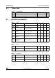
VNS1NV04DP-E Package and PCB thermal data Table 10. Thermal parameters Area/island (cm2) 0.07 R1 = R7 (°C/W) 0.02 R2 = R8 (°C/W) 2 R3 = R9 (°C/W) 11 R4 = R10 (°C/W) 30 R5 = R11 (°C/W) 25 R6 = R12 (°C/W) 100 R13 = R14 (°C/W) 250 C1 = C2 = C7 = C8 (W.s/°C) 0.0005 C3 = C9 (W.s/°C) 0.02 C4 = C10 (W.s/°C) 0.035 C5 = C11 (W.s/°C) 0.2 C6 = C12 (W.s/°C) 0.4 Doc ID 17344 Rev 3 0.15 0.3 0.6 87.5 74.2 62.6 0.51 0.65 0.
Package and packing information VNS1NV04DP-E 5 Package and packing information 5.1 ECOPACK® packages In order to meet environmental requirements, ST offers these devices in different grades of ECOPACK® packages, depending on their level of environmental compliance. ECOPACK® specifications, grade definitions and product status are available at: www.st.com. ECOPACK® is an ST trademark. 5.2 SO-8 package information Figure 34.
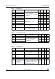
VNS1NV04DP-E Package and packing information Table 11. SO-8 mechanical data Symbol Millimeters Min. Typ. A Max. 1.75 A1 0.10 A2 1.25 b 0.28 0.48 c 0.17 0.23 D(1) 4.80 4.90 5.00 E 5.80 6.00 6.20 E1(2) 3.80 3.90 4.00 e 0.25 1.27 h 0.25 0.50 L 0.40 1.27 L1 k 1.04 0° ccc 8° 0.10 1. Dimensions D does not include mold flash, protrusions or gate burrs. Mold flash, potrusions or gate burrs shall not exceed 0.15 mm in total (both side). 2.
Package and packing information 5.3 VNS1NV04DP-E SO-8 packing information Figure 35. SO-8 tube shipment (no suffix) B Base Q.ty Bulk Q.ty Tube length (± 0.5) A B C (± 0.1) C A 100 2000 532 3.2 6 0.6 All dimensions are in mm. Figure 36. SO-8 tape and reel shipment (suffix “TR”) REEL DIMENSIONS Base Q.ty Bulk Q.ty A (max) B (min) C (± 0.2) F G (+ 2 / -0) N (min) T (max) 2500 2500 330 1.5 13 20.2 12.4 60 18.4 All dimensions are in mm.
VNS1NV04DP-E 6 Revision history Revision history Table 12. Document revision history Date Revision Changes 09-Jun-2008 1 Initial release. 02-Apr-2010 2 Changed template. Updated Table 17: Turn-on current slope (part 1/2). 20-Sep-2013 3 Updated Disclaimer.
VNS1NV04DP-E Please Read Carefully: Information in this document is provided solely in connection with ST products. STMicroelectronics NV and its subsidiaries (“ST”) reserve the right to make changes, corrections, modifications or improvements, to this document, and the products and services described herein at any time, without notice. All ST products are sold pursuant to ST’s terms and conditions of sale.