
Datasheet


Electrical specifications VNS1NV04DP-E
6/24 Doc ID 17344 Rev 3
2 Electrical specifications
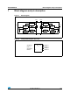
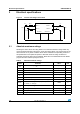
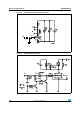
Figure 3. Current and voltage conventions
2.1 Absolute maximum ratings
Stressing the device above the rating listed in the “Absolute maximum ratings” table may
cause permanent damage to the device. These are stress ratings only and operation of the
device at these or any other conditions above those indicated in the operating sections of
this specification is not implied. Exposure to Absolute maximum rating conditions for
extended periods may affect device reliability. Refer also to the STMicroelectronics SURE
program and other relevant quality document.
DRAIN 1
INPUT 1
SOURCE 2
I
IN1
V
IN1
INPUT 2
I
IN2
SOURCE 1
DRAIN 2
V
IN2
I
D2
I
D1
V
DS1
V
DS1
R
IN1
R
IN2
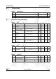
Table 2. Absolute maximum ratings
Symbol Parameter Value Unit
V
DSn
Drain-source voltage (V
INn
= 0 V) Internally clamped V
V
INn
Input voltage Internally clamped V
I
INn
Input current +/-20 mA
R
IN MINn
Minimum input series impedance 330
I
Dn
Drain current Internally limited A
I
Rn
Reverse DC output current -3 A
V
ESD1
Electrostatic discharge (R = 1.5 K, C = 100 pF) 4000 V
V
ESD2
Electrostatic discharge on output pins only
(R = 330 , C = 150 pF)
16500 V
P
tot
Total dissipation at T
c
=25°C 4 W
T
j
Operating junction temperature Internally limited °C
T
c
Case operating temperature Internally limited °C
T
stg
Storage temperature -55 to 150 °C