
Datasheet


Electrical specifications VNS1NV04DP-E
8/24 Doc ID 17344 Rev 3
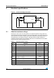
Table 7. Switching
(1)
1. T
j
= 25 °C, unless otherwise specified.
Symbol Parameter Test conditions Min. Typ. Max. Unit
t
d(on)
Turn-on delay time
V
DD
=15V; I
D
=0.5A;
V
gen
=5V; R
gen
=R
IN MIN
= 330
(see Figure 4)
70 200 ns
t
r
Rise time 170 500 ns
t
d(off)
Turn-off delay time 350 1000 ns
t
f
Fall time 200 600 ns
t
d(on)
Turn-on delay time
V
DD
=15V; I
D
=0.5A
V
gen
=5V; R
gen
=2.2K
(see Figure 4)
0.25 1 µs
t
r
Rise time 1.3 4 µs
t
d(off)
Turn-off delay time 1.8 5.5 µs
t
f
Fall time 1.2 4 µs
(dI/dt)
on
Turn-on current slope
V
DD
=15V; I
D
=1.5A
V
gen
=5V; R
gen
=R
IN MIN
= 330
5A/µs
Q
i
Total input charge
V
DD
=12V; I
D
= 0.5 A; V
IN
=5V
I
gen
= 2.13 mA (see Figure 7)
5nC
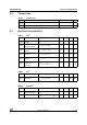
Table 8. Source Drain diode
(1)
1. T
j
= 25 °C, unless otherwise specified.
Symbol Parameter Test conditions Min. Typ. Max. Unit
V
SD
(2)
2. Pulsed: pulse duration = 300µs, duty cycle 1.5%.
Forward on voltage I
SD
= 0.5 A; V
IN
=0V - 0.8 - V
t
rr
Reverse recovery time
I
SD
= 0.5 A; dI/dt = 6 A/µs
V
DD
=30V; L=200µH
(see Figure 5)
- 205 - ns
Q
rr
Reverse recovery charge - 100 - nC
I
RRM
Reverse recovery current - 0.75 - A
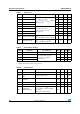
Table 9. Protections
(1)
1. -40 °C < T
j
< 150 °C, unless otherwise specified.
Symbol Parameter Test conditions Min. Typ. Max. Unit
I
lim
Drain current limit V
IN
=5V; V
DS
=13V 1.7 3.5 A
t
dlim
Step response current
limit
V
IN
=5V; V
DS
=13V 2 µs
T
jsh
Overtemperature
shutdown
150 175 200 °C
T
jrs
Overtemperature reset 135 °C
I
gf
Fault sink current V
IN
=5V; V
DS
=13V; T
j
=T
jsh
10 15 20 mA
E
as
Single pulse
avalanche energy
Starting T
j
=25°C; V
DD
=24V
V
IN
=5V R
gen
=R
IN MIN
= 330
L=50mH
(see Figure 6 and Figure 8)
55 mJ