
Datasheet


74VHC132
2/11
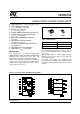
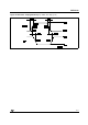
Figure 2: Input Equivalent Circuit Table 2: Pin Description
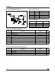
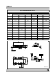
Table 3: Truth Table
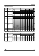
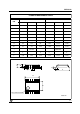
Table 4: Absolute Maximum Ratings
Absolute Maximum Ratings are those values beyond which damage to the device may occur. Functional operation under these conditions is
not implied
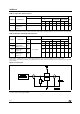
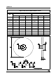
Table 5: Recommended Operating Conditions
PIN N° SYMBOL NAME AND FUNCTION
1, 4, 9, 12 1A to 4A Data Inputs
2, 5, 10, 13 1B to 4B Data Inputs
3, 6, 8, 11 1Y to 4Y Data Outputs
7 GND Ground (0V)
14
V
CC
Positive Supply Voltage
ABY
LLH
LHH
HLH
HHL
Symbol Parameter Value Unit
V
CC
Supply Voltage
-0.5 to +7.0 V
V
I
DC Input Voltage
-0.5 to +7.0 V
V
O
DC Output Voltage -0.5 to V
CC
+ 0.5
V
I
IK
DC Input Diode Current
- 20 mA
I
OK
DC Output Diode Current
± 20 mA
I
O
DC Output Current
± 25 mA
I
CC
or I
GND
DC V
CC
or Ground Current
± 50 mA
T
stg
Storage Temperature
-65 to +150 °C
T
L
Lead Temperature (10 sec)
300 °C
Symbol Parameter Value Unit
V
CC
Supply Voltage
2 to 5.5 V
V
I
Input Voltage
0 to 5.5 V
V
O
Output Voltage 0 to V
CC
V
T
op
Operating Temperature
-55 to 125 °C