
Datasheet


74VHC132
4/11
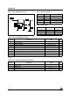
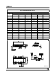
Table 8: Capacitive Characteristics
1) C
PD
is defined as the value of the IC’s internal equivalent capacitance which is calculated from the operating current consumption without
load. (Refer to Test Circuit). Average operating current can be obtained by the following equation. I
CC(opr)
= C
PD
x V
CC
x f
IN
+ I
CC
/4 (per gate)
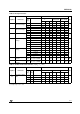
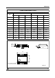
Table 9: Dynamic Switching Characteristics
1) Worst case package.
2) Max number of outputs defined as (n). Data inputs are driven 0V to 5.0V, (n-1) outputs switching and one output at GND.
3) Max number of data inputs (n) switching. (n-1) switching 0V to 5.0V. Inputs under test switching: 5.0V to threshold (V
ILD
), 0V to threshold
(V
IHD
), f=1MHz.
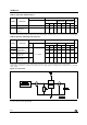
Figure 3: Test Circuit
C
L
=15/50pF or equivalent (includes jig and probe capacitance)
R
T
= Z
OUT
of pulse generator (typically 50Ω)
Symbol Parameter
Test Condition Value
Unit
T
A
= 25°C
-40 to 85°C -55 to 125°C
Min. Typ. Max. Min. Max. Min. Max.
C
IN
Input Capacitance
610 10 10pF
C
PD
Power Dissipation
Capacitance
(note 1)
16 pF
Symbol Parameter
Test Condition Value
Unit
V
CC
(V)
T
A
= 25°C
-40 to 85°C -55 to 125°C
Min. Typ. Max. Min. Max. Min. Max.
V
OLP
Dynamic Low
Voltage Quiet
Output (note 1, 2)
5.0
C
L
= 50 pF
0.3 0.8
V
V
OLV
-0.8 -0.3
V
IHD
Dynamic High
Voltage Input
(note 1, 3)
5.0 3.5 V
V
ILD
Dynamic Low
Voltage Input
(note 1, 3)
5.0 1.5 V