A5972D Up to 1.5 A step down switching regulator for automotive applications Features ■ Qualified following the AEC-Q100 requirements (see PPAP for more details) ■ 1.5A DC output current ■ Operating input voltage from 4 V to 36 V ■ 3.3 V / (±2%) reference voltage ■ Output voltage adjustable from 1.
Contents A5972D Contents 1 2 Pin settings . . . . . . . . . . . . . . . . . . . . . . . . . . . . . . . . . . . . . . . . . . . . . . . . 4 1.1 Pin connection . . . . . . . . . . . . . . . . . . . . . . . . . . . . . . . . . . . . . . . . . . . . . . 4 1.2 Pin description . . . . . . . . . . . . . . . . . . . . . . . . . . . . . . . . . . . . . . . . . . . . . . 4 Electrical data . . . . . . . . . . . . . . . . . . . . . . . . . . . . . . . . . . . . . . . . . . . . . . 5 2.1 Maximum ratings . . .
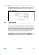
A5972D Contents 8.3 Thermal considerations . . . . . . . . . . . . . . . . . . . . . . . . . . . . . . . . . . . . . . 21 8.4 Short-circuit protection . . . . . . . . . . . . . . . . . . . . . . . . . . . . . . . . . . . . . . . 23 8.5 Application circuit . . . . . . . . . . . . . . . . . . . . . . . . . . . . . . . . . . . . . . . . . . . 25 8.6 Positive buck-boost regulator . . . . . . . . . . . . . . . . . . . . . . . . . . . . . . . . . . 28 8.7 Negative buck-boost regulator . . . . . . . . .
Pin settings A5972D 1 Pin settings 1.1 Pin connection Figure 2. 1.2 Pin description Table 1. 4/37 Pin connection (top view) Pin description N Pin Description 1 OUT Regulator output. 2,3,6,7 GND Ground. 4 COMP 5 FB 8 VCC E/A output for frequency compensation. Feedback input. Connecting directly to this pin results in an output voltage of 1.23 V. An external resistive divider is required for higher output voltages. Unregulated DC input voltage.
A5972D Electrical data 2 Electrical data 2.1 Maximum ratings Table 2. Absolute maximum ratings Symbol Value Unit 40 V V V V8 Input voltage V1 OUT pin DC voltage OUT pin peak voltage at Δt = 0.1 μs -1 to 40 -5 to 40 I1 Maximum output current int. limit. V4, V5 Analog pins PTOT Power dissipation at TA ≤ 70 °C TJ TSTG 2.2 Parameter 4 V 1.
Electrical characteristics 3 A5972D Electrical characteristics TJ = -40 °C to 125 °C, VCC = 12 V, unless otherwise specified. Table 4. Electrical characteristics Symbol VCC RDS(on) IL fSW Parameter Test condition Operating input voltage range Min Typ Max Unit 36 V 0.250 0.5 Ω 1.8 2.5 3 2 2.5 3 212 250 280 kHz 100 % 1.
A5972D 4 Datasheet parameters over the temperature range Datasheet parameters over the temperature range The 100% of the population in the production flow is tested at three different ambient temperatures (-40 °C; +25 °C, +125 °C) to guarantee the datasheet parameters inside the junction temperature range (-40 °C; +125 °C). The device operation is so guaranteed when the junction temperature is inside the (-40 °C; +150 °C) temperature range.
Functional description 5 A5972D Functional description The main internal blocks are shown in the device block diagram in Figure 3. They are: ● A voltage monitor circuit which checks the input and the internal voltages. ● A fully integrated sawtooth oscillator with a frequency of 250 kHz ± 15%, including also the voltage feed forward function and an input/output synchronization pin. ● Two embedded current limitation circuits which control the current that flows through the power switch.
A5972D 5.2 Functional description Voltages monitor An internal block continuously senses the Vcc, Vref and Vbg. If the voltages go higher than their thresholds, the regulator begins operating. There is also a hysteresis on the VCC (UVLO). Figure 4. 5.3 Internal circuit Current protection The A5972D features two types of current limit protection: pulse-by-pulse and frequency foldback. The schematic of the current limitation circuitry for the pulse-by-pulse protection is shown in Figure 5.
Functional description Figure 5. 5.4 A5972D Current limitation circuitry Error amplifier The voltage error amplifier is the core of the loop regulation. It is a transconductance operational amplifier whose non inverting input is connected to the internal voltage reference (1.235 V), while the inverting input (FB) is connected to the external divider or directly to the output voltage. The output (COMP) is connected to the external compensation network.
A5972D Functional description diode can be considered a high value capacitor and this produces a very high peak current, responsible for numerous problems: ● Spikes on the device supply voltage that cause oscillations (and thus noise) due to the board parasites. ● Turn ON overcurrent leads to a decrease in the efficiency and system reliability. ● Major EMI problems. ● Shorter freewheeling diode life.
Additional features and protection A5972D 6 Additional features and protection 6.1 Feedback disconnection If the feedback is disconnected, the duty cycle increases towards the maximum allowed value, bringing the output voltage close to the input supply. This condition could destroy the load. To avoid this hazardous condition, the device is turned OFF if the feedback pin is left floating. 6.
A5972D 7 Closing the loop Closing the loop Figure 7.
Closing the loop 7.1 A5972D Error amplifier and compensation network The output L-C filter of a step-down converter contributes with 180 degrees phase shift in the control loop. For this reason a compensation network between the COMP pin and GROUND is added. The simplest compensation network together with the equivalent circuit of the error amplifier are shown in Figure 8. RC and CC introduce a pole and a zero in the open loop gain.
A5972D Closing the loop whereas the zero is defined as: Equation 5 1 F Z1 = -----------------------------------2 • π • Rc • Cc FP1 is the low frequency which sets the bandwidth, while the zero FZ1 is usually put near to the frequency of the double pole of the L-C filter (see below). FP2 is usually at a very high frequency. 7.
Closing the loop A5972D If the damping coefficient δ is very close to zero, the roots of the equation become a double root whose value is ωn. Similarly for ALC the poles can usually be defined as a double pole whose value is: Equation 11 1 F PLC = --------------------------------------------2 • π • L • C OUT 7.
A5972D Closing the loop Example: Considering RC = 4.7 kΩ, CC = 22 nF and CP = 220 pF, the poles and zeroes of A0 are: FP1 = 9 Hz FP2 = 150 kHz FZ1 = 1.5 kHz If L = 33 µH, COUT = 100 µF and ESR = 80mΩ, the poles and zeroes of ALC become: FPLC = 3.3 kHz FZESR = 19.89 kHz Finally R1 = 5.6 kΩ and R2 = 3.3 kΩ. The gain and phase bode diagrams are plotted respectively in Figure 9 and Figure 10. Figure 9. Module plot Figure 10.
Application information A5972D 8 Application information 8.1 Component selection ● Input capacitor The input capacitor must be able to support the maximum input operating voltage and the maximum RMS input current. Since step-down converters draw current from the input in pulses, the input current is squared and the height of each pulse is equal to the output current.
A5972D Application information Where VF is the freewheeling diode forward voltage and VSW the voltage drop across the internal PDMOS. Considering the range DMIN to DMAX, it is possible to determine the max IRMS going through the input capacitor. Capacitors that can be considered are: Electrolytic capacitors: These are widely used due to their low price and their availability in a wide range of RMS current ratings.
Application information Table 7. A5972D Output capacitor selection Manufacturer Series Cap value (µF) Rated voltage (V) ESR (mΩ) Sanyo POSCAP(1) TAE 100 to 470 4 to 16 25 to 35 THB/C/E 100 to 470 4 to 16 25 to 55 TPS 100 to 470 4 to 35 50 to 200 KEMET T494/5 100 to 470 4 to 20 30 to 200 Sprague 595D 220 to 390 4 to 20 160 to 650 AVX 1. POSCAP capacitors have some characteristics which are very similar to tantalum.
A5972D 8.2 Application information Layout considerations The layout of switching DC-DC converters is very important to minimize noise and interference. Power-generating portions of the layout are the main cause of noise and so high switching current loop areas should be kept as small as possible and lead lengths as short as possible. High impedance paths (in particular the feedback connections) are susceptible to interference, so they should be as far as possible from the high current paths.
Application information A5972D compensate for the losses in the overall application. For this reason, the switching losses related to the RDSON increases compared to an ideal case. ● Switching losses due to turning ON and OFF.
A5972D Application information RDS(on) has a typical value of 0.25 @ 25 °C and increases up to a maximum value of 0.5. @ 150 °C. We can consider a value of 0.4 Ω. TSW is approximately 70 ns. IQ has a typical value of 2.5 mA @ VIN = 12 V. The overall losses are: Equation 25 2 P TOT = R DSON • ( I OUT ) • D + V IN • I OUT • T SW • F SW + V IN • I Q = 2 = 0.4 • 1.5 • 0.3 + 12 • 1.5 • 70 • 10 –9 3 • 250 • 10 + 12 • 2.5 • 10 –3 ≅ 0.
Application information A5972D In short-circuit conditions VOUT is negligible so during TOFF the voltage across the inductor is very small as equal to the voltage drop across parasitic components (typically the DCR of the inductor and the VFW of the free wheeling diode) while during TON the voltage applied the inductor is instead maximized as approximately equal to VIN.
A5972D Application information Figure 14. Short-circuit current VIN = 24 V Figure 15. Short-circuit current VIN = 36 V 8.5 Application circuit Figure 16 shows the evaluation board application circuit, where the input supply voltage, VCC, can range from 4 V to 36 V and the output voltage is adjustable from 1.235 V to 6.3 V due to the voltage rating of the output capacitor,.
Application information A5972D Figure 16. Evaluation board application circuit L1 33uH A5972D Table 9. Component list Reference 26/37 Part number Description Manufacturer C1 GRM42-2 X7R 475K 50 4.7 µF, 50 V Murata C2 POSCAP 6TAE330ML 330 µF, 6.3 V Sanyo C3 C1206C470J5GAC 47 pF, 5%, 50 V KEMET C4 C1206C223K5RAC 22 nF, 10%, 50 V KEMET R1 5.6 kΩ, 1%, 0.1 W 0603 Neohm R2 3.3 kΩ, 1%, 0.1 W 0603 Neohm R3 22 kΩ, 1%, 0.
A5972D Application information Figure 17. PCB layout (component side) Figure 18. PCB layout (bottom side) Figure 19.
Application information 8.6 A5972D Positive buck-boost regulator The device can be used to implement a step-up/down converter with a positive output voltage. The output voltage is given by: Equation 32 D V OUT = V IN ⋅ ------------1–D where the ideal duty cycle D for the buck boost converter is: Equation 33 V OUT D = ----------------------------V IN + V OUT However, due to power losses in the passive elements, the real duty cycle is always higher than this.
A5972D Application information Figure 20. Positive buck-boost regulator 8.7 Negative buck-boost regulator In Figure 21, the schematic circuit for a standard buck-boost topology is shown. The output voltage is: Equation 37 D V OUT = – V IN ⋅ ------------1–D where the ideal duty cycle D for the buck boost converter is: Equation 38 – V OUT D = ----------------------------V IN – V OUT The considerations given in Section 8.7 for the real duty cycle are still valid here.
Application information A5972D Figure 21. Negative buck-boost regulator 8.8 Compensation network with MLCC at the output MLCCs (multiple layer ceramic capacitor) with values in the range of 10 µF-22 µF and rated voltages in the range of 10 V-25 V are available today at relatively low cost from many manufacturers. These capacitors have very low ESR values (a few mΩ) and thus are occasionally used for the output filter in order to reduce the voltage ripple and the overall size of the application.
A5972D Application information Figure 22.
Typical characteristics 9 A5972D Typical characteristics Figure 23. Line regulation Figure 24. Load regulation Vo (V) 3.312 Vcc = 12V Vo = 3.3V 3.308 3.304 Tj = 25°C 3.3 3.296 3.292 3.288 3.284 Tj = 125°C 3.28 3.276 0 0.5 1 1.5 Io (A) Figure 25. Output voltage vs junction temperature Figure 26. Switching frequency vs junction temperature Figure 27. Quiescent current vs junction Figure 28.
A5972D Typical characteristics Figure 29. Junction temperature vs output current Figure 30. Junction temperature vs output current Figure 31. Efficiency vs output current Figure 32.
Package mechanical data 10 A5972D Package mechanical data In order to meet environmental requirements, ST offers these devices in different grades of ECOPACK® packages, depending on their level of environmental compliance. ECOPACK® specifications, grade definitions and product status are available at: www.st.com. ECOPACK is an ST trademark.
A5972D Package mechanical data Table 10. SO-8 mechanical data mm. inch Dim. Min Typ Max Min Typ Max A 1.35 1.75 0.053 0.069 A1 0.10 0.25 0.004 0.010 A2 1.10 1.65 0.043 0.065 B 0.33 0.51 0.013 0.020 C 0.19 0.25 0.007 0.010 (1) 4.80 5.00 0.189 0.197 E 3.80 4.00 0.15 0.157 D e 1.27 0.050 H 5.80 6.20 0.228 0.244 h 0.25 0.50 0.010 0.020 L 0.40 1.27 0.016 0.050 k 0° (min.), 8° (max.) ddd 0.10 0.004 1.
Revision history 11 A5972D Revision history Table 11.
A5972D Please Read Carefully: Information in this document is provided solely in connection with ST products. STMicroelectronics NV and its subsidiaries (“ST”) reserve the right to make changes, corrections, modifications or improvements, to this document, and the products and services described herein at any time, without notice. All ST products are sold pursuant to ST’s terms and conditions of sale.