STE100P 10/100 FAST ETHERNET 3.3V TRANSCEIVER 1 DESCRIPTION Figure 1. Package The STE100P, also referred to as STEPHY1, is a high performance Fast Ethernet physical layer interface for 10Base-T and 100Base-TX applications. It was designed with advanced CMOS technology to provide a Media Independent Interface (MII) for easy attachment to 10/100 Media Access Controllers (MAC) and a physical media interface for 100Base-TX of IEEE802.3u and 10Base-T of IEEE802.3.
STE100P 2.
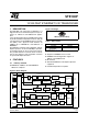
STE100P 3 PIN ASSIGNMENT DIAGRAM rx_clk gnde/i rx_er/rxd4 tx_er/txd4 tx_clk tx_en txd0 txd1 txd2 txd3 col crs mdint vcce/i cfg1 cfg0 Figure 4.
STE100P Table 2. Pin Description (continued) Pin No. Name Type Description 52 tx_er I Transmit Coding Error. The MAC asserts this input when an error has occurred in the transmit data stream. When the STE100P is operating at 100 Mbps, the STE100P responds by sending invalid code symbols on the line. In Symbol (5B) Mode this pin functions as txd4. 51 43 44 46 47 rxd4 rxd3 rxd2 rxd1 rxd0 O Receive Data. The STE100P drives received data on these outputs, synchronous to rx_clk.
STE100P Table 2. Pin Description (continued) Pin No. Name Type Description 15 iref O Reference Resistor connecting pin for reference current, directly connect a 5KΩ ± 1% resistor to Vss. 38 ledr10 I/O LED display for 10Ms/s link status. This pin will be driven on continually when 10Mb/s network operating speed is detected. The pull-up/pull-down status of this pin is latched into the PR20 bit 7 during power up/reset. 37 ledtr 36 ledl I/O LED display for Link Status.
STE100P Table 2. Pin Description (continued) Pin No. Name Type 5 4 3 2 1 mf0 mf1 mf2 mf3 mf4 I Description Multi-Function pins. Each mf pin internally drives different configuration functions. The functions of the five mf inputs are as shown in the table below. The logic level of mf0-4 will determine the value that the affected bits will have upon reset of the STE100P. The operating functions of cfg0, cfg1, and fde change depending on the state of mf0 (Auto-Negotiation enabled or disabled).
STE100P 5 HARDWARE CONTROL INTERFACE 5.1 Operating Configurations The Hardware Control Interface consists of the MF<4:0>, CFG <1:0> and FDE input pins as well as the LED/PAD pins. This interface is used to configure operating characteristics of the STE100P. The Hardware Control Interface provides initial values for the MDIO registers, and then passes control to the MDIO Interface. Individual chip addressing via the LED/PAD pins allows multiple STE100P devices to share the MII interface.
STE100P 6 REGISTERS AND DESCRIPTORS DESCRIPTION There are 11 registers with 16 bits each supported for the STE100P. These include 7 basic registers which are defined according to the clause 22 “Reconciliation Sublayer and Media Independent Interface” and clause 28 “Physical Layer link signaling for 10 Mb/s and 100 Mb/s Auto-Negotiation on twisted pair” of IEEE802.3u standard. In addition, there are 4 special registers for advanced chip control and status information. 6.1 Register List Table 4.
STE100P Table 5. Register Descriptions (continued) Bit # Name Descriptions Default Val RW Type 11 PDEN Power-down mode control. 1: Power-down mode is selected. Setting this bit puts the STE100P into power-down mode. During the power-down mode, TXP/TXN and all LED outputs are 3-stated, and the MII interface is isolated. 0 R/W 10 ISOEN 0 – Normal operation. 1 – Isolate PHY from MII. Setting this control bit isolates the STE100P from the MII, with the exception of the serial management inter-face.
STE100P Table 5. Register Descriptions (continued) Bit # Name Descriptions Default Val RW Type 6 MFPS MF Preamble Suppression 1 =Accepts management frames with pre-amble suppressed. 0 = Will not accept management frames with preamble suppressed. The value of this bit is controlled by bit 1 of PR20. Its default of 1 indicates that the SFEPHY1 accepts management frame without preamble. A minimum of 32 preamble bits are required following power-on or hardware reset.
STE100P Table 5. Register Descriptions (continued) Bit # Name Descriptions Default Val RW Type 13 RF Remote Fault function. 1: with remote fault function. 0 R/W 12,11 --- Reserved 10 FC Flow Control function Ability. 1:supports PAUSE operation of flow control for full duplex link. 1 R/W 9 T4 100BASE-T4 Ability. Always 0: since STE100P doesn’t have 100BASE-T4 ability. 0 RO 8 TXF 100Base-TX Full duplex Ability. 1: with 100Base-TX full duplex ability.
STE100P Table 5. Register Descriptions (continued) Bit # Name Descriptions Default Val RW Type 5 LP10H Link Partner’s 10Base-T Half Duplex ability. 0: link partner without 10Base-T ability. 1: link partner with 10Base-T ability. 0 RO 4~0 LPSF Link partner select field. Default 00001=IEEE 802.3. 00001 RO Reserved 0 RO Parallel detection fault. 0: no fault detected. 1: a fault detected via parallel detection function. 0 RO/LH* Link Partner’s Next Page ability.
STE100P Table 5. Register Descriptions (continued) Bit # Name 3 ANAR 2 PDF 1 ANPR 0 REF Descriptions Default Val RW Type Interrupt source of Auto-Negotiation Acknowledge Received. 0: there is no link code word received. 1: link code word is receive from link partner. 0 RO/LH* Interrupt source of Parallel Detection Fault. 0: there is no parallel detection fault. 1: parallel detection is fault. 0 RO/LH* Interrupt source of Auto-Negotiation Page Received.
STE100P Table 5. Register Descriptions (continued) Bit # Name Descriptions Default Val RW Type 11, 10 --- 9 ENRLB Enable remote loop-back function. 1: enable 0 R/W 8 ENDCR Enable DC restoration. 0: disable DC restoration. 1: enable DC restoration. 1 R/W 7 ENRZI Enable the conversions between NRZ and NRZI. 0: disable the data conversion between NRZ and NRZI. 1: enable the data conversion of NRZI to NRZ in receiving and NRZ to NRZI in transmitting.
STE100P Table 5. Register Descriptions (continued) 7 Bit # Name Descriptions Default Val RW Type 7~3 PAD4:0 PHY Address [4:0]: The values of the PAD[4:0] pins are latched to this register at power-up/reset. The first PHY address bit transmitted or received is the MSB of the address (bit 4). A station management entity connected to multiple PHY entities must know the appropriate address of each PHY.
STE100P Data conversion of Parallel to Serial, NRZ to NRZI, NRZI to MLT3: After scrambled, the transmission data with 5B type in 25MHz will be converted to serial bit stream in 125MHz by the parallel to serial function. After serialized, the transmission serial bit stream will be further converted from NRZ to NRZI format. This NRZI conversion function can be bypassed, if the bit 7 of PR19 register is cleared as 0.
STE100P 7.5 Loop-back Operation The STE100P provides internal loop-back option for both the 100Base-TX and 10Base-T operations. Setting bit 14 of PR0 register to 1 can enable the loop-back option. In this loop-back operation, the txp/txn and rxp/rxn lines are isolated from the media. The STE100P also provides remote loop-back operation for 100Base-TX operation. Setting bit 9 of PR19 register to 1 enables the remote loop-back operation.
STE100P 7.9 LED Display Operation The STE100P provides 5 LED pins, the detail descriptions about the operation are described in the PIN Description section, and as follows. ■ Speed LED: 100Mbps(on) or 10Mbps(off) ■ Receive LED: Blinks at 10Hz when receiving, but not colliding ■ Transmit LED: Blinks at 10Hz when transmitting, but not colliding ■ Link LED: On when 100M or 10M link ok ■ Collision LED: Blinks at 20Hz to indicate a collision 7.10 Reset Operation There are two ways to reset the STE100P.
STE100P Note: The above LED connections are recommended for setting a Logic Level 1 or Logic Level 0 on the STE100P LED/PHY Address pins, for determining PHY address. 7.11 Preamble Suppression Preamble suppression mode in the STEPHY1 is indicated by a one in bit six of the PR1 Register. If it is determined that all PHY devices in the system support preamble suppression, then a preamble is not necessary for each management transaction.
STE100P 8 ELECTRICAL SPECIFICATIONS AND TIMINGS Table 6. Absolute Maximum Ratings Parameter Value Supply Voltage(Vcc) -0.5 V to 7.0 V Input Voltage -0.5 V to VCC + 0.5 V Output Voltage -0.5 V to VCC + 0.5 V Storage Temperature -65 °C to 150 °C(-85°F to 302°F) Ambient Temperature (-40)°C to +85°C) ESD Protection 2000V Table 7. General DC Specifications Symbol Parameter Test Condition Min. Typ. Max. Units 3.15 3.3 3.
STE100P Table 8. AC Specifications Symbol Parameter Test Condition Min. Typ. Max. Units 45 50 55 % X1 Specifications TX1d X1 Duty Cycle TX1p X1 Period TX1t X1 Tolerance TX1CL 30 ns ±50 PPM X1 Load Capacitance 18 pF 10Base-T Normal Link Pulse (NLP) Timings Specifications TNPW NLP Width 10Mbps TNPC NLP Period 10Mbps 100 8 ns 24 ms Max. Units Figure 8. Normal Link Pulse timings Tnpw Tnpc Table 8. AC Specifications Symbol Parameter Test Condition Min. Typ.
STE100P Figure 9. Fast Link Pulse timing Tflcpp Tflcpd Tflpw Tflbw Tflbp Table 8. AC Specifications Symbol Parameter Test Condition Min. Typ. Max. Units 1.
STE100P Figure 10. MII Management Clock Timing t1 t2 t3 MDC t4 t5 MDIO(I) t6 MDIO(O) Table 8. AC Specifications Symbol Parameter Test Condition Min. Typ. Max.
STE100P Figure 11. MII Receive Timing Table 8. AC Specifications Symbol Parameter Test Condition Min. Typ. Max. Units MII Transmit Timing Specification t1 TX-ER,TX-EN,TXD[3:0] Setup to TX-CLK Rise 10 — ns t2 TX-ER,TX-EN,TXD[3:0] Hold After TX-CLK Rise 0 25 ns Figure 12.
STE100P Table 8. AC Specifications Symbol Parameter Test Condition Min. Typ. Max. Units Receive Timing Specification Rt1 Rt2 Rt3 Rt4 Receive Frame to Sampled Edge of RX-DV (100 Mbits/s) — 300 ns Receive Frame to Sampled Edge of RX-DV (10 Mbits/s) — 4 us Receive Frame to CRS High (100Mbits/s) — 250 ns Receive Frame to CRS High (10 Mbits/s) — 3.
STE100P Table 8. AC Specifications Symbol Parameter Test Condition Min. Typ. Max.
STE100P Figure 15. 100BaseT Transmit Timing TXP Table 9. Parameter Sym Min Typ Max Units TXD, TX_EN, TX_ER Setup to TX_CLK High t2A 10 - - ns TXD, TX_EN, TX_ER Hold from TX_CLK High t2B 5 - - ns TX_EN sampled to CRS asserted t2C - 30 40 ns TX_EN sampled to CRS de-asserted t2D - 40 160 ns TX_EN sampled to TXP out (Tx latency) t2E 60 100 140 ns BT is the duration of one bit as transferred to and from the MAC and is the reciprocal of the bit rate.
STE100P Figure 16. 10Base-T Half Duplex Transmit Timing TXP Table 10.
STE100P 9 PACKAGE INFORMATION In order to meet environmental requirements, ST offers these devices in ECOPACK® packages. These packages have a Lead-free second level interconnect. The category of second Level Interconnect is marked on the package and on the inner box label, in compliance with JEDEC Standard JESD97. The maximum ratings related to soldering conditions are also marked on the inner box label. ECOPACK is an ST trademark. ECOPACK specifications are available at: www.st.com. Figure 17.
STE100P Table 11. Revision History Date Revision January 2004 15 Rev. A12 June 2003 has been migrated from ST-PRESS to EDOCS. June 2004 16 Changed the Style-sheet on the Rev. A13. August 2004 17 Wrong package corrected. September 2004 18 Due to Rev. 17 content was partially wrong. Now fixed. February 2005 19 Added part number “E-STE100P” (ECOPACK).
STE100P Information furnished is believed to be accurate and reliable. However, STMicroelectronics assumes no responsibility for the consequences of use of such information nor for any infringement of patents or other rights of third parties which may result from its use. No license is granted by implication or otherwise under any patent or patent rights of STMicroelectronics. Specifications mentioned in this publication are subject to change without notice.