
Datasheet


STE100P
6/31
5
4
3
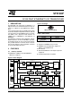
2
1
mf0
mf1
mf2
mf3
mf4
I Multi-Function pins. Each mf pin internally drives different configuration
functions. The functions of the five mf inputs are as shown in the table below.
The logic level of mf0-4 will determine the value that the affected bits will have
upon reset of the STE100P. The operating functions of cfg0, cfg1, and fde change
depending on the state of mf0 (Auto-Negotiation enabled or disabled). Table 2
shows the relationship between cfg0, cfg1 and fde.
6fde IFull-Duplex Enable.
When A/N is enabled, fde determines full-duplex advertisement capability in
combination with cfg0 and cfg1. (See Table 2)
When A/N is disabled, fde directly affects full-duplex operation and determines
the value of PR0 bit 8 (Full/Half Duplex Mode Select).
When fde is High, full-duplex is enabled and PR0:8 = 1.
When fde is Low, full-duplex is disabled and PR0:8 = 0.
Digital Power Pins
39, 45, 62 vcce, vcce/i
25, 40, 50 gnde, gnde/i
Analog Power Pins
9, 13, 16, 17, 22 vcca
7, 10, 14, 20, 24 gnda
Table 2. Pin Description (continued)
Pin No. Name Type Description