
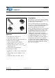
Datasheet


Electrical characteristics L4931
10/38 DocID4340 Rev 18
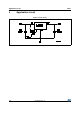
(Refer to the test circuits, T
A
= -40 to 125 °C, C
I
= 0.1 µF, C
O
= 2.2 µF unless otherwise
specified).
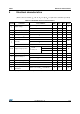
Table 4. L4931Cxx27-TRY (automotive-grade) electrical characteristics
Symbol Parameter Test conditions Min. Typ. Max. Unit
V
O
Output voltage
I
O
= 5 mA, V
I
= 4.7 V, T
A
= 25 °C 2.646 2.7 2.754
V
I
O
= 5 mA, V
I
= 4.7 V 2.592 2.808
V
I
Operating input voltage I
O
= 250 mA 20 V
I
out
Output current limit T
A
= 25 °C 300 mA
ΔV
O
Line regulation V
I
= 3.4 to 20 V, I
O
= 0.5 mA 20 mV
ΔV
O
Load regulation V
I
= 3.6 V, I
O
= 0.5 to 250 mA 38 mV
I
d
Quiescent current
ON mode
V
I
= 3.6 to 20 V, I
O
= 0 mA 1
mA
V
I
= 3.6 to 20 V, I
O
= 250 mA 6
OFF mode V
I
= 6 V 100 µA
SVR Supply voltage rejection
I
O
= 5 mA
V
I
= 4.6 ± 1 V
T
A
= 25 °C
f = 120 Hz 74
dBf = 1 kHz 71
f = 10 kHz 55
eN Output noise voltage B = 10 Hz to 100 kHz, T
A
= 25 °C 50 µV
V
d
Dropout voltage
I
O
= 250 mA, T
A
= 25 °C 0.4 0.6 V
I
O
= 250 mA 0.82 V
V
IL
Control input logic low 0.82 V
V
IH
Control input logic high 2 V
I
I
Control input current V
I
= 6 V, V
C
= 6 V, T
A
= 25 °C 10 µA
C
O
Output bypass
capacitance
ESR = 0.1 to 10 Ω, I
O
= 0 to 250 mA,
T
A
= 25 °C
210 µF