
Datasheet


L6234 Thermal data
Doc ID 1107 Rev 10 5/16
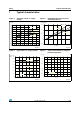
3 Thermal data
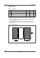
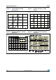
Figure 3. Printed Heatsink
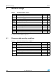
Table 3. Thermal data
Symbol Parameter DIP16+2+2 PowerSO20 Unit
R
th j-pin
Thermal resistance, junction to pin 12
(1)
1. The thermal resistance is referred to the thermal path from the dissipating region on the top surface of the
silicon chip, to the points along the four central pins of the package, at a distance of 1.5 mm away from the
stand-offs.
– °C/W
R
th j-amb1
Thermal resistance, junction to ambient 40
(2)
2. If a dissipating surface, thick at least 35 mm, and with a surface similar or bigger than the one shown in
Figure 3, is created making use of the printed circuit. Such heatsinking surface is considered on the bottom
side of an horizontal PCB (worst case).
– °C/W
R
th j-amb2
Thermal resistance, junction characteristics) to
ambient
50
(3)
3. If the power dissipating pins (the four central ones), as well as the others, have a minimum thermal
connection with the external world (very thin strips only) so that the dissipation takes place through still air
and through the PCB itself. It is the same situation of note 2, without any heatsinking surface created on
purpose on the board.
– °C/W
R
th j-case
Thermal resistance junction-case – 1.5 °C/W
!-V